Unlike before, when computers, tablets, PlayStations, and other electronic devices have to be big to accommodate all their functions, the 21st-century technology consumers place a lot of emphasis on portability.
The continued reduction in the size of electronic devices, which has further enhanced portability, is made possible by the advent of HDI PCBs. Now, devices can be smaller without a loss in function or quality. In case you're yearning to know the origin, uses, and applications of the HDI PCB. Just keep reading, and have your curiosity addressed.
Contents
- 1、What is HDI PCB?
- 2、Why Opt for HDI PCB?
- ♦ Compact Design
- ♦ Improved Signal Transmission
- ♦Unmatched Versatility
- ♦Very Reliable
- ♦Pocket-Friendly
- 2.1: Benefits of HDI PCB
- 2.2: Advantages of HDI PCB
- 3、How HDI Differs from Standard PCBs
- 3.1: HDI VS Standard PCB: The Differences
- 3.2: Tabular Differences between HDI PCB and Standard PCB
- 4、Are There Challenges with HDI PCBs?
- 4.1: Demerits of HDI PCB
- 5、HDI Applications
- • Healthcare
- • Automotives
- • Tablets and Smartphone
- • Wearable Technology
- • Aerospace and Military
- 6、The Future of HDI PCB
- 7、Conclusion
Special Offer: Get $100 off your order!
Please email [email protected] for details.
1、What is HDI PCB?
HDI, an acronym for High-Density Interconnect, refers to the PCB type with so many interconnections, but which does not take up much space. The implication of this is that circuit boards can now be as small as a designer wants since the constituents can be miniaturized to occupy little space. Despite this reduction, the functionality stays uncompromised.
Stated differently, any PCB with around one hundred and twenty to one hundred and sixty pins occupying a square inch is qualified to be called an HDI PCB. The two major components of a typical HDI design are versatile routing and component placement. It was because of the HDI that Micro vias technology became renowned. This technology gave birth to denser circuitries using Micro vias, blind vias, and buried vias.
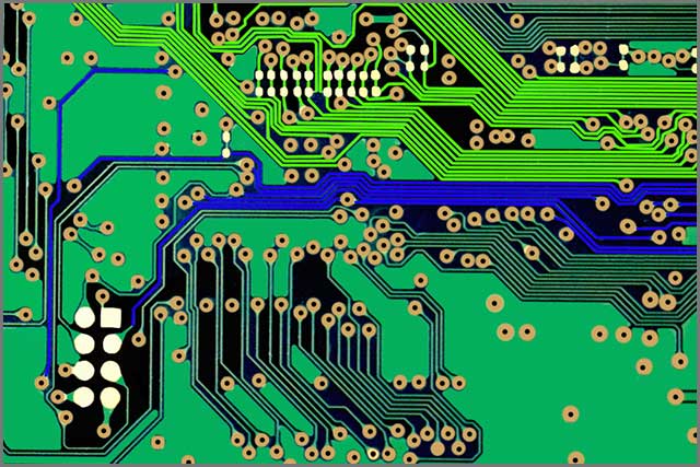 Image 1: Electronic circuit board showing High-Density Interconnect PCBs
2、Why Opt for HDI PCB?
There are several reasons why HDI PCB is a choice any electronics designer would want to make. First, it is lighter and smaller than the contemporary PCB. Second, it helps to save costs. Furthermore, because the path length is reduced, signal transmission with HDI is greatly improved. Perhaps you are still wondering if opting for HDI PCB is the way to go at this time and age. Here are some salient reasons that can answer the questions in the affirmative.
♦ Compact Design
With the compatibility that HDI offers electronic designs these days, it's hard to say no to it. With HDI, you have the trio of Micro vias, blind vias, and buried vias in one small space, leading to a more portable electronic output.
♦ Improved Signal Transmission
Two technologies that HDI adopts (blind via and via-in-pad) make it possible for designers to bring circuit components closer than before, and this, in turn, reduces the path length of the signal. The result of this is an enhanced signal transmission.
♦Unmatched Versatility
An electronics designer may sometimes wish to achieve several aims such as reliability, weight, and space reduction, including enhanced performance in one output. All of these are achievable either independently or at once with HDI PCB.
♦Very Reliable
A good PCB must be resistant-to a degree- too harsh environmental conditions. Failure to meet this condition may amount to a constant fault, which would affect the manufacturer’s credibility. HDI implements stacked vias, and this delivers an extra shield to it from extreme conditions.
♦Pocket-Friendly
Because of the possible reduction in PCB's component layer with HDI without affecting the functionality, it has become easy to carry around anywhere, anytime. For example, only four layers of HDI PCB can implement all the functions of an eight-layer standard PCB.
2.1: Benefits of HDI PCB
• Interference and noise are both minimized, and this ensures an enhanced EMC
• More circuitry density compared to the standard PCB
• Trace and lead inductances significantly reduced
• Greater pad density connection
• Smaller capture pads and vias
• Significant signal transmission improvement owing to reduced signal paths
• Aspect ratio is relatively smaller (1:1)
• The micro vias laser drilling is quite accurate
• The Micro vias and buried/blind vias are within the range of four to six ml.
2.2: Advantages of HDI PCB
• By reducing the number and count of PCB, HDI helps to save cost
• It is now possible to greatly reduce the weight and size of electronic products. thanks to HDI
• Devices can now perform better because HDI ensures shorter tracking, and this results in inductance reduction. A reduced inductance means improved electrical performance.
• Similarly, embedded resistors and capacitors are connected in one layer by HDI's Micro vias. It shortens the mass and distance of the conductive substance. Of course, when this happens, electrical performance becomes improved.
Special Offer: Get $100 off your order!
Please email [email protected] for details.
3、How HDI Differs from Standard PCBs
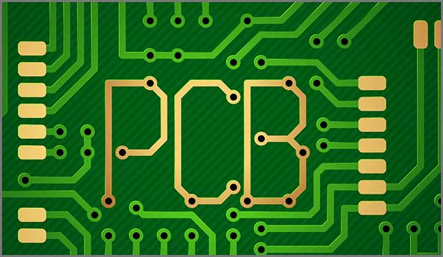 Image 2: circuit board inscription with PCB holes
At the center of the differences between HDI PCB and Standard PCBs is HDI supplies' improved signal integrity. It’s not that hard to figure out how this can be so. It reduces the stray inductance and capacitance that can degrade signal performance in HDI PCBs. Of course, other differences include the obvious portability that HDI offers. The weight is lighter, and electronics no longer have to consume much space.
3.1: HDI VS Standard PCB: The Differences
HDI {high density interconnector} is just a circuit board that contains a higher line distribution density. It is a higher density interconnector board that uses the micro-blind buried hole. This circuit board comprises an interior and exterior layer line. HDI uses the metallization and drilling process inside the hole for the connection of every layer.
Generally, High density interconnects a lamination process produces boards. As a result, the more layers added, the board’s technical grade increases. Normally, the method of producing HDI is mainly a lamination method. For instance, two technology layers or more are used for high-order HDI. It also integrates the PCB advanced technology like; direct laser drilling, plating holes, and stacking holes.
As the PCB density increases above its eight-layer board, it can construct in HDI at a lower cost than traditional pressing methods, which is complex. HDI board makes it quite easy to use sophisticated packaging technology. Also, it facilitates HDI electrical functioning, which makes signal precision higher than the conventional PCB. Furthermore, Its boards are more suitable for heat conduction: Radio Frequency Interference, electrostatic discharge, electromagnetic interference, and much more.
3.2: Tabular Differences between HDI PCB and Standard PCB
Most electronic devices keep on leaning towards high precision and density. The ‘high’ in its makeup shows the machine’s improvement in performance and its size reduction. The HDI technology makes sure that end-product designs are portable and, at the same time, meet the high standards of efficiency and electronic performance. For instance, HDI boards are used by present-day popular devices such as automotive, electronics notebook, computers, digital cameras, mobile phones, etc.
However, with PCB, you can avoid the manual wiring, and the electrical device that adopts it can be mounted or inserted automatically. They can also be soldered and detected automatically. As a result of its quality, cost reduction, maintenance is more comfortable, and labor productivity increases. The table below further gives the differences between the two.
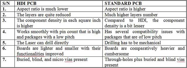 Image 3: The difference between the HDI PCB and Standard PCB
4、Are There Challenges with HDI PCBs?
 Image 4: Printed circuit board
Of course, due to the recent and advanced technologies, there are bound to be challenged.
Moreover, the manufacturing of PCB and HDI are constantly evolving. As electronic technology, tablet computers, wearable devices, and intelligent mobile phones develop rap, day; it brings challenges to HDI PCBs, especially since its direction goes towards functional and multifunctional capacity. Due to the increased integration rate in the communication devices, the manufacturing and design of PCB get more obvious.
The margins for HDI veneer left by manufacturers get smaller. These manufacturing and design constraints increase the design complexity. It also destroys the time required for the plywood to join. As a result, there is a direct negative impact on output time. Furthermore, high-density package assembly, PCB assembly will result in tomb bump, more solid bridge, shift, and many other things. The present detection system comes with certain limitations, and as a result, doing a high-density test is difficult. Also, the device used for pin spacing is tiny, which increases the problems of repairers.
4.1: Demerits of HDI PCB
The demerits are as follows;
• This technology is still at its evolving stage
• The yield is lower
• You can achieve the same technique in other ways
• The equipment needed is expensive
• Its plating process seems quite difficult
• The use of blind vias is not economical, mainly when used in high density and performance systems. They are not like through-hole vias, which you can use for either low or high-performance PCB systems.
• The usage of blind HDI PCBs results in higher cost, unlike the through-hole vias. The reason is due to the additional tasks carried out on the board.
• The multi-layers required for HDI manufacturing needs adequate materials.
• Via holes tend to be sensitive
• There is fiberglass in the standard-pregs' makeups, which changes the laser route and produces the laser's wrong shape via holes.
5、HDI Applications
The application of HDI spreads towards several areas such as healthcare, automotive, tablets and smartphones, wearable technology, and the military. The individual relevance of HDI in these fields is review below.
• Healthcare
The medical industry is getting a positive impact of HDI. The medical gadgets used by healthcare are normally HDI. For instance, devices like; imaging equipment, lab, and implants, which are tiny devices.
• Automotives
The automobile industries are also attracted by the tiny sized HDI PCBs most especially since it provides more room within the car.
• Tablets and Smartphone
Every one of the Smartphone you use today is HDI PCBs with Every Layer Interconnection Construction. HDI PCBs use for creating light and tiny compact electronic devices.
• Wearable Technology
Devices like the apple watch, VR headsets, and other wearable devices come from HDI PCBs.
• Aerospace and Military
The military has also incorporated HDI through their communication and strategic equipment devices. HDI PCBs are compatible with a dangerous and harsh environment, making them perfect for military and aerospace applications.
 Image 5: Magnetic Resonance Imaging device made of HDI PCB
6、The Future of HDI PCB
HDI PCBs take technology to its highest order. It plays an important role in the manufacturing of electronic devices. This technology brings satisfaction to the greatest challenges with its innovations. HDI PCB is a consumer-driven technology. Most especially since consumers are looking for devices that will allow them to work anywhere and anytime comfortably. As a result, this technology's future is a very bright one since the demand will continue to get higher and not lower.
 Image 6: CPU chipset on printed circuit board
7、Conclusion
The coming of HDI PCBs has made the hardware of the digital world very easy. It brought about a reduction in the size of electronic gadgets and the manufacturing of important electronic devices. It is now very easy to use your Smartphone to watch your favorite programs. Even laptops and computers are no longer heavy and ugly, and you can comfortably and conveniently use them anywhere. To be precise, HDI PBCs have facilitated human convenience by minimizing electronic devices. We believe at this point. You have a general idea of how HDI PCBs work. The only thing you should do now is to register on the OurPCB website and place an order. The desired HDI PCB boards will arrive at your doorstep in the shortest possible time-frame!
Special Offer: Get $100 off your order!
Please email [email protected] for details.