


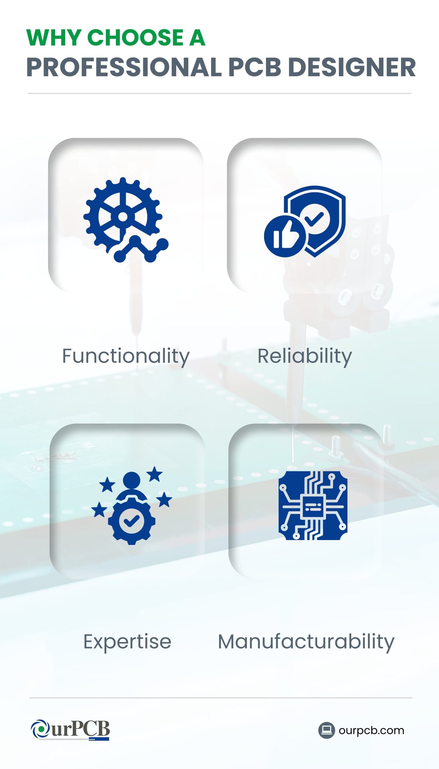

PCB design and fabrication service providers such as OurPCB can craft designs that are optimal for the manufacturing process. They can accurately translate schematics into fully functional boards.
Using professional PCB design services grants you access to experienced professionals. This minimizes the risk of errors, faults, and poor designs that are unlikely to perform well in the long run. Moreover, you can hold these professionals accountable if something goes wrong during the design or PCB manufacturing process.
Professional PCB Design services put you in touch with licensed professionals who understand the more specialized technical aspects of PCB design and fabrication. For instance, they can determine the best trace width and spacing to minimize electromagnetic interference (EMI). They can also organize components in a way that fully optimizes electromagnetic compatibility (EMC) and ensures strong signal integrity.
Professional design and fabrication service providers understand all requirements necessary to produce designs that meet manufacturing tolerances and specifications. By using OurPCB for your PCB design needs, you can reduce costs and the risk of reworks.

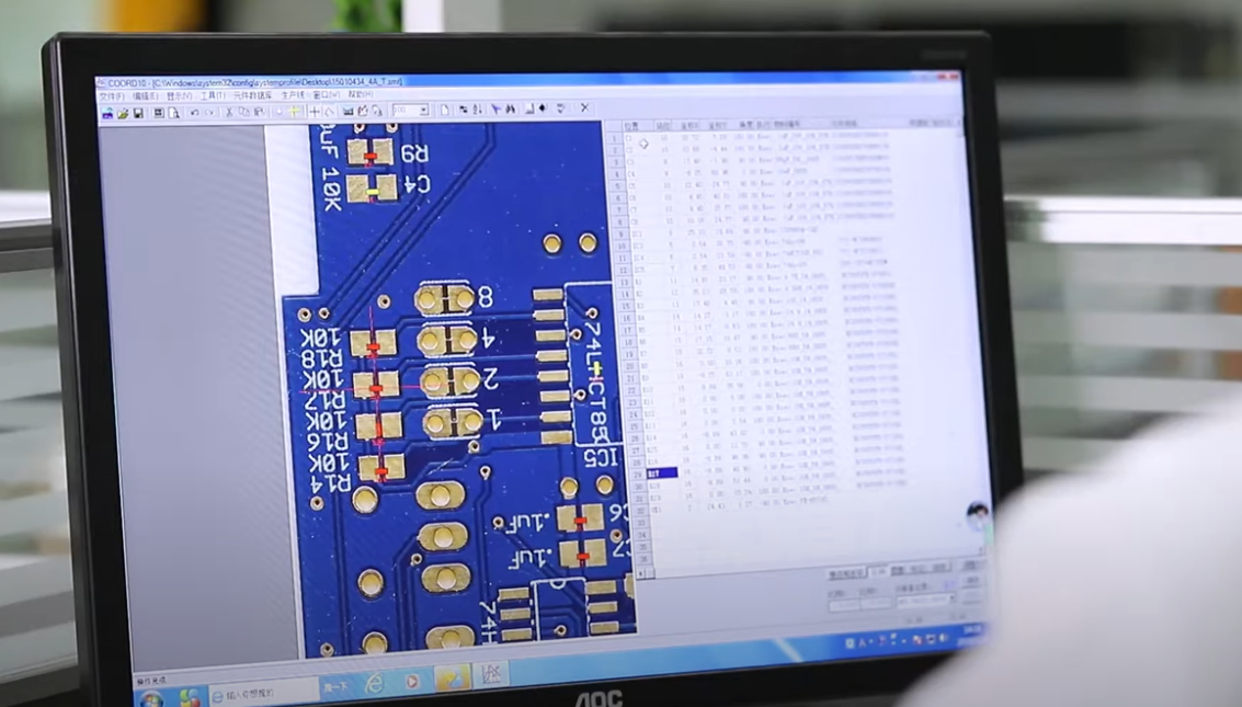
Our expert engineers craft precise and detailed schematic diagrams, no matter the complexity of your project.
Leveraging advanced tools such as Altium Designer, Cadence, Eagle, and KiCAD, we produce reliable and efficient PCB layouts tailored to your needs.
We provide end-to-end firmware development services to enhance the functionality of embedded systems seamlessly.
Custom software and app solutions according to your specifications.
We specialize in creating innovative algorithm solutions for a wide range of applications, including image processing and data analysis challenges.
Rapid prototyping and optimized designs with 3D printing and enclosure design expertise.

Mon-Fri: 24 hours,
Sat: 9am-6pm, GMT+8
Reach us at
[email protected]
24 hours online
+86-199-30589219
Mon-Fri: 24 hours,
Sat: 9am-6pm, GMT+8

