Visas are required on any PCB to establish the connection patterns between the multiple layers of a multi-layered board. Vias are often covered with different materials to conduct electrical signals and dissipate the heat in the process.
Did you know that you can tent vias with copper to make them more conductive? Do you know the difference between different tenting and plugging techniques?
We have prepared this helpful guide to give answers to all your questions. Our discussion will cover the various processes used to fill vias and the advantages associated with each of them.
Contents
- 1、 What is Tenting Via
- 1.1 What is Plugging Via
- 1.2 Tenting Vias VS. Plugged Vias
- 2、 Solder-Filled Vias
- 2.1 Copper-Filled Vias
- 2.2 Conductive Vs. Non-Conductive Filled Vias
- Conductive Fill
- Non-Conductive Fill
- 2.3 Solder Mask Over Vias
- 2.4 Vias Plated Shut with Copper
- 3、 Better PCBs in Eagle
- 3.1 Eagle Trace Width
- 3.2 Eagle Via Size
- 3.3 tenting via--Eagle Design Rules
- 3.4 tenting via--Eagle Design Rule Check
- 4、 tenting via--Vias Not Covered
- tenting via--Pros
- tenting via--Cons
- 5、tenting via--Via in Pad
- 6、tenting via--Via Plugging
- 7、tenting via--Conclusion
Special Offer: Get $100 off your order!
Please email [email protected] for details.
1、 What is Tenting Via
Vias can be negligible in size, but they are crucial parts of a printed circuit board (PCB). Vias interconnect the copper traces on different layers of a multi-layered PCB.
There are different types of vias, and drilling holes on the PCB makes all of them. You will never find any component lead passing through the hole of a visa.
A visa may be tented or left exposed — a tenting of a via means that a solder mask has been used to cover the via over the hole in the shape of a tent or a skin.
Earlier, manufacturers had difficulty tenting the vias using liquid photo-imageable (LPI) solder masks. But with the introduction of the dry film solder mask, the process has become much more comfortable.
Tenting a PCB reduces the number of exposed conductive pads and the chances of shorts arising from solder bridging. It also protects the vias from corrosion and external elements.
When dealing with SMT pads, tenting is useful to lessen past migration from the SMD elements when the vias are designed at the end of places.
Tenting is also ideal for vias close to SMT pads, reducing the chances of being short during reflow. Sometimes, the tented via is again given a coat of solder mask.
1.1 What is Plugging Via
Plugging is a process where the vias are entirely plugged with a material such as a solder mask or fill. After that, the manufacturer applies the LPI mask over the plug.
The via barrel doesn't receive any surface finish under this plugged-via process. They were filling vias to guarantee that a visa had been tested thoroughly.
You must perform some extra steps to plug a via during fabrication. The via size must be considered, and the via isn't given any surface finish.
During curing, you must also control the ascent rate to neutralize all volatiles. If you cannot control the rise, the solder mask can smear on the surface while the assembly reflow is carried out.
Vias can be plugged with conductive and non-conductive fill. You can use a non-conductive epoxy material or solder mask to ensure complete coverage of the vias and toroids. It will ensure that you don't create poor or weak solder joints in BGA SMD pads.
tenting via
At present, the BGA packages are becoming tighter. It is difficult to place the vias using standard 'dog-bone area patterns for carrying signals to the outer layers.
For this reason, the vias are drilled right on the pads of the BGA footprint and enable you to route signals easily.
The via holes have to be fully plugged for this process. After that, the plugged via is plated with copper and flattened to be aligned with other copper features.
Some surface-mounted devices on a PCB can produce excessive heat, which needs to be conducted away for proper functioning. For this reason, thermal vias are often plugged with conductive fills.
The fills are metallic and transfer the heat to the other side of the board. The fillings also cut back the resistance of the traces and were applied to chips that carry high amounts of current.
That, in turn, lowers the voltage drop between the SMD and the voltage source pins.
1.2 Tenting Vias VS. Plugged Vias
Tenting Vias is a process where the solder mask is used to cover the vias. Different tenting procedures, such as screen coating, spray, and curtain, can be used.
But the methods may not be enough to provide a complete tenting of the via. For example, squirt and specific strategies may not suffice to wrap the via on both sides.
The process of screen coating also has some limitations to hole size and board thickness.
Plugged vias are useful in many scenarios, such as BGA design, where the vias are generally placed very close to the SMD pads. In such scenarios, plugged vias come to the rescue.
While fabrication, steps ensure that the masked plugging or the non-conductive fills form a complete seal and tents the annular ring. The process guarantees that the vias are 100% tented and filled.
While plugging, the mask clearance is first removed from the via. Then the holes are filled based on the design parameters of the PCB.
The via plugging is carried out based on the standards developed by the IPC.
You have got the hang of raw via tenting and plugging concepts. We will take the discussion further with solder-filled vias in the next chapter.
 Image 1: Tenting Via
2、 Solder-Filled Vias
2.1 Copper-Filled Vias
Vias enable the transfer of signals from one side of the board to the other. The manufacturer applies a layer of copper over the PCB, which provides its conductive properties and establishes a connection between the layers connected by holes.
The copper plating is adequate to transmit electric signals, but the manufacturer may use another conductive material to fill the gaps for added capacity.
Copper increases the thermal conductivity of the board, carrying heat away from sensitive PCB components and dissipating to the other side of the board. It reduces the chances of developing defects and increases the lifespan of the PCB.
Copper-filled vias are also ideal for applications that require large amounts of current to pass from one side of the board to the other.
The conductive nature of copper enables high-current signals to pass without putting stress on the PCB. It makes copper field vias suitable for high-voltage applications.
Copper-filled vias come with increased production costs but become necessary when high stability is required.
2.2 Conductive Vs. Non-Conductive Filled Vias
Conductive Fill
Conductively filled vias are metallic and conduct heat effectively. They are used to fill a via when it transfers a large amount of current or heat to the other side of the board.
Conductive fills are ideal for situations that involve a lot of heat, such as under the chips, which are prone to overheating.
The process leads to one drawback- a difference in the Coefficient of Thermal Expansion (CTE) between the conductive fill and the surrounding laminate.
The walls and pads can break in-between as the metallic filler expand more quickly than the surrounding laminate.
For this reason, this process is unsuitable for some applications, such as Via in Pad, where the filling is done to ensure the durability of the copper plating covering the hole.
Non-Conductive Fill
Many people believe that vias filled with non-conductive fills are unable or can pass a weak electric signal from one side to another.
But this doesn't hold as the hole barrels of all the vias on the board are plated with copper, which comes with conductive properties.
Only the non-conductive fills have replaced the atmospheric air in the barrels.
You may use this process to ensure that solder or other contaminants don't end you entering the holes. It is also suitable to render structural support for copper pads over the vias.
2.3 Solder Mask Over Vias
Vias can cover many materials, and the solder mask is one of the most common. The solder mask can be applied to the holes in many ways, such as vias closed by the solder mask on both ends and vias left open on one end.
Sometimes the vias are left open on both sides, and the solder mask covers only the annular rings. The type of plating you will need depends on the nature of the application and your purpose.
You can apply the solder mask over vias during the assembly process. First, the whole surface of the board is coated with solder mask ink and then left to dry.
The ink in the solder mask can be hardened by exposing it to UV light since the material is UV sensitive.
Some ink parts are not exposed to UV light according to design specifications. They remain soft, and you can wash them off using a 1% alkalic solution.
 Image 2:Tenting Via
2.4 Vias Plated Shut with Copper
You can find this method of filling in older legacy and military equipment. Vias plated shut with copper provide a conductive fill and are more reliable than tenting vias with non-conductive filling and applying them to a plate.
The copper filling also makes for a solid core. You also get an even surface to plate the via, producing high-quality finished assembly. The process also prevents the solder from dispersing and affecting the solder joint at the assembly level.
The process has some limitations. You will find it very difficult to plate the whole barrel smoothly.
The upper and lower parts of the via will be plated faster while some air r liquid may be trapped in the middle.
For vias to be plated with copper, the holes should be small. The copper used to fill a via will also plate all the copper components on the board, increasing the total copper. Let's take an example-
You know that 1 oz of copper is equivalent to 1.4 mils. The amount of copper you will need to fill a via of 8 mils is 2.8 oz. Plating covers both sides of the barrel, so eight mil/2, or 4.
Now 4 mil/1.4 or 2.85 oz will be the extra amount of copper compared to existing copper features such as traces and vias.
The total weight of the copper range between 2.3 to 4 oz, which is too much for boards with size restrictions.
Now we will find out how to make better PCBs in Eagle.
Special Offer: Get $100 off your order!
Please email [email protected] for details.
3、 Better PCBs in Eagle
3.1 Eagle Trace Width
Trace widths are essential considerations in PCB design and determine the amount of current you can pass without overheating and damaging the board.
You can set different trace widths in your Eagle PCB design by changing the width and accessing the trace width in the DRC rules.
3.2 Eagle Via Size
The default via size in Eagle is taken to be 0.6mm. You can change the size according to the needs of your project and application.
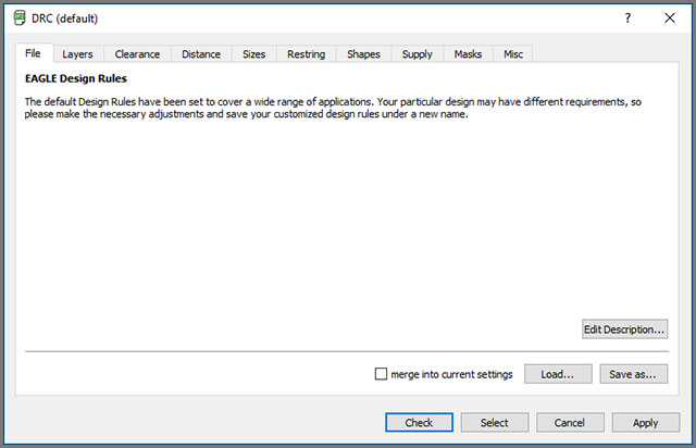 Image 3: Tenting Via
3.3 tenting via--Eagle Design Rules
The Design Rules in Eagle software lets you set the values and parameters of your PCB design. For example, you can select the trace widths of the layers, the size of the vias, and the pads. You can edit the Design rules as you find them suitable.
3.4 tenting via--Eagle Design Rule Check
The Eagle Design Rule Check enables you to validate your PCB design according to the physical limitations of the manufacturing process.
You can set a range of boundaries related to component spacing, trace width, and use the DRC tool to ensure all your design specifications match the requirements.
You can find the DRC tool in your Eagle Control Panel.
The next chapter will explore the pros and cons of vias not covered.
4、 tenting via--Vias Not Covered
The uncovered through holes do not have any solder mask on the annular ring and the via barrel. The standard PCB fabrication process only involves applying surface finish material to the holes.
tenting via--Pros
The process is ideal for high-current traces and can conduct heat effectively. It also solders the via holes for the application of wave soldering.
Since the through-holes are uncovered, you can carry outboard testing by accessing both sides of the board.
tenting via--Cons
Leaving vias exposed can lead to many disadvantages. Vias can corrode from exposure to the environment and get damaged.
They can also come in contact with other surfaces, increasing the risks of shorts.
The molten solder can pass out of the holes and create solder balls and splashes during wave soldering.
Some materials used to clean the PCB can also get stuck in the exposed vias and corrode the copper plating.
The visa can also get damaged while testing, breaking in the net.
Now let's find out a bit about Via in Pad.
 Image 4: Tenting Via
5、tenting via--Via in Pad
PCBs and BGA (Ball Grid Arrays) have been getting smaller daily, increasing the importance of Via in Pad technology.
The technology doesn't use the traditional 'dog-bone land pattern when transferring signals from the BGA footprint, which sends signals to other layers. Instead, the vias are drilled right into the BGA footprint pads.
Via in Pads provides benefits over through-hole or blind holes by offering improved precision. You can also achieve space savings as the process creates higher-density PCBs.
Via in Pads also dissipates heat effectively and makes room for better thermal management. It also reduces the PCB area and provides an even surface with the other components.
We have almost come to the end of our discussion. Let's take a look via plugging before wrapping things up.
 Image 5: Tenting Via
6、tenting via--Via Plugging
Via plugging is necessary when you completely tent the holes connecting the different layers of the PCB. Generally, a non-conductive fill promotes the vias, such as a solder mask.
You can also go for conductive fillers such as copper to increase the conductivity of the board. The annular ring is also covered with a show used to seal the whole barrel.
The solder mask protects the copper traces from corrosion, oxidation, and solder bridging.
They are also more resistant to electrical shorts and physical damage. Plugged vias become important for space-restricting applications such as BGA design.
 Image 6: Tenting Via
7、tenting via--Conclusion
Tenting vias serve many important purposes and come as standard processes under PCB fabrication.
You can expose vias or plug them completely using conductive and non-conductive materials. Sometimes, the BGA design uses Via in Pad technology with space limitations.
We can manufacture high-quality PCBs via tenting and plugs. Our manufacturing techniques ensure that vias are created according to your design specifications with the plating you prefer.
Get in touch with our team to learn more about our high standards via the tenting process and order your batch of PCBs.
Special Offer: Get $100 off your order!
Please email [email protected] for details.