For most designers, the desire to create a PCB whose land pattern meets the industry standard and does not cause problems during repairs is crucial. You might occasionally have an overcrowded land pattern, more so if you are a new designer and wish to have every component on your board.
This article is essential if you desire to produce circuit boards whose land patterns meet the industry standard. If you wish to get more knowledge on the Land pattern, take time, and enjoy reading the content.

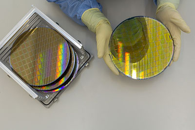
( A land pattern display on a circuit board)
Contents
- 1. What is the land pattern
- So, why is it essential?
- 2. land-pattern vs. Footprint
- 2.1 What is the Footprint?
- 2.2 How do we distinguish between Land pattern and Footprint?
- 3. Inline With IPC-7351 Standard Design
- 3.1 What is IPC-7351?
- 3.2 Other matters of IPC-7351 standard
- 3.3 Description of land pattern size design
- 4. What is the Best Software for Land Pattern Design
- Schematic symbol:
- The package that meets IPC requirements:
- 5. Our Recommended Land Pattern
- Summary:
Special Offer: Get $100 off your order!
Please email [email protected] for details.
1. What is the land pattern
A land pattern is the arrangement of pads on a circuit board. Primarily, a land pattern attaches and connects the electronic component on a circuit board depending on the layout and the design of the board. It is also important to note that land patterns should always match with the arrangements of lead.
So, why is it essential?
Designing the land part is essential since it ensures reliability by determining the solder joint. It makes it easier to identify defects in the solder joint. Besides, it plays a broad role in repairing, testing, and cleaning the solder joint.
2. land-pattern vs. Footprint
2.1 What is the Footprint?
In the PCB world, the word footprint refers to a pattern that resembles the electronic component soldered there, irrespective of the connector you will use. An impression reaches your physical foot. When you stand on the sand, you will notice some dent that looks like your foot.
2.2 How do we distinguish between Land pattern and Footprint?
In PCB assembly, the word footprint and land pattern might mean the same thing and sometimes might differ for several reasons. You need to realize that when someone uses these words, there is a distinction. The observable difference between the two terms is that a footprint resembles a person’s foot. When you press your leg in soft sand, you notice the impression left behind. For a land pattern, it is the size of the pads. It resembles a part that is already there, which you design into PCB.
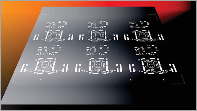
(Stencils on a PCB board that display PCB footprint)
Special Offer: Get $100 off your order!
Please email [email protected] for details.
3. Inline With IPC-7351 Standard Design
3.1 What is IPC-7351?
Universally, PCBs must conform to specific standards formulated by the Institute for Interconnecting and Packaging Electronic Circuits. It is a trade organization that sets up various standards that protect both manufacturers and consumers from ensuring safer PCB products.
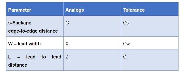
The IPC -7351 refers to the set dimensions you must use to create a land pattern essential for PCB footprints. These dimensions include:
- pad spacing (labeled as G),
- the pad width (labeled X),
- the pad end to end dimension (labeled Z).
They will help in the accommodation of component spacing, thereby preventing solder defects.
You need to understand that there is a need to calculate the G, X, and Z. the first thing we will know about is the formula to use;
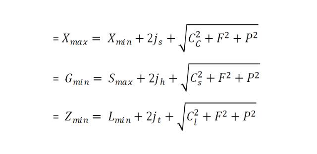
(The IPC -7351 recommended formulas)
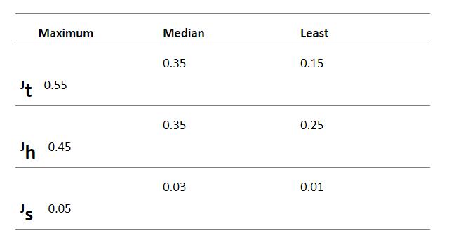
When designing, you need to ensure that the land pattern can accommodate solder fillet on every lead’s edge. Here you use three J values as shown above. For parameter S, you measure the component’s outer edge while measuring the end of the charges. The minimum and maximum dimensions mean that you need to include dimensional tolerance. You use the letter C to show patience for each size.
The table below summarizes all the parameters
3.2 Other matters of IPC-7351 standard
One world CAD library is what the IPC-7351 bar has createdDoing, increasing the consistency of the PCB footprint. When it comes to print, it is more than the drawings done on paper. It will include the PCB land pattern, solder mask, component outline, and silkscreen markings when you use CAD software. When designing your land pattern, when you use CAD software, it is careful to recommend sizes. Ensure you do not violate the standards set.
3.3 Description of land pattern size design
There is a need to confirm the size of the land pattern. It will help you to decide on the best amount of solder that you use. The size of the solder you use to mount a capacitor plays a broad role in influencing capacitor directs on the printed circuit. Therefore, you need to make enough consideration when deciding.
When designing your land pattern and your amount of solder is much, you cause trouble to the capacitor. It may easily crack. It necessitates the need to set up the right size of the land pattern for the solder amount. Again, when the solder amount is little than required, the terminal’s strength will not be enough. Your capacitor may drop from the printed wire board. It also affects the reliability of the circuit.
So, what are the recommendable size to use;
When it comes to the actual standard size, creepage distance should be 2.5 or even more. For the dimension, a suitably certified capacitor should be 3.0 to 3.5 mm. To prevent electrical discharge, you need to ensure a slit between the lands or cleaning.
4. What is the Best Software for Land Pattern Design
Identifying the right software for your land pattern design will give any designer an easy time identifying and creating your footprint.
Using the component footprint generator can reduce the design time, using CAD software for innovation, the tools we need to use:
Schematic symbol:
These are the essential diagrams that are simplified. It shows the components and electrical connections that are in a circuit. There is always the need to learn more about the component symbols before using the schematic. Some of the characters need to learn are the capacitor, power sources, capacitors, potentiometers, resistors, etc.
If you long to use the schematic symbol, then you made the right choice. You will be able to save on time for the design and also on the cost. Using the tools gives you the confidentiality that you are doing the right thing and the correct dimensions.
The package that meets IPC requirements:
If you do not long to make those calculations, a component footprint generator is the best place to start. You need to use an IPC compliant footprint. Here you will need to use the package that has CAD tools. You only need to have some design strategies to use. If you wish to work this more straightforward way, choose Ceramic Quad Flatpack. It is the best package that you will not struggle with following the procedures.
This package is the best to choose since it will provide you an excellent format for a high pin count. It also includes a top and bottom section, which is essential for your case. The package also works with or without a heat sink, which is a great deal for you.
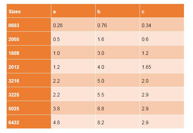
5. Our Recommended Land Pattern
Here is the most recommended land pattern that our experts have seen to be the best for use. It would be best if you choose the right dimension for you based on the size you require. All units are in (mm).
Summary:
Understanding and designing the land pattern will help you determine solder joint strength and identify solder defects. You also get to choose the solder joint’s reliability and easily clean it in the right way. It is an important way of meeting the required standard by the state.
By reading the content, we trust that you will understand and practice the ideal PCB footprints. It is our pleasure to see you here on our platform. It is always essential to learn more about PCB design. If you wish to learn more, feel free to get in touch with us. We have other valuable materials that will be of great help in your career. There is a need to keep learning day in day out since technology is growing fast.
Special Offer: Get $100 off your order!
Please email [email protected] for details.