A PCB is a device that helps support and connect different electrical components. We will delve into the more technical details later on. For starters, we need to address the importance of PCBs to professionals.
PCBs are often prone to design flaws and functional disabilities. It can be problematic when it comes to professional work.
There is also a safety risk that comes hand in hand with faulty PCBs. The following sections will explain all the problems you can encounter while working with PCB electronics and the solutions.
Contents
- 1、What is PCB Electronics?
- 1.1 Resistors
- 1.2 Integrated circuits
- 1.3. Silkscreen
- 1.4 Vias
- 1.5 Capacitors
- 1.6 Diodes
- 1.7 FR4
- 2、What are the PCB Electronics Characteristics You Can Choose?
- 2.1 Through Hole
- 2.2 Surface Mount
- 3、What are the Common PCB Electronics Problems?
- 3.1. What are Plating Voids?
- 3.2. What problems can arise for not using DFM?
- 3.3. What is Inadequate Copper to edge clearance?
- 4、Having Silver in PCB Electronics: The Problems
- 5、Should you worry about missing solder masks between pads?
- 6、Why are Acid Traps Worrisome in PCB Electronics?
- 7、What Electromagnetic PCB Electronics issues can you face?
- 8、Conclusion
1、What is PCB Electronics?
Did you know that PCB electronics has a layout similar to that of lasagna? PCBs typically consist of layers. These are, namely, Substrate or Fiberglass, Copper, Soldermask, and Silkscreen. These layers are fixed in place using lamination, industrial adhesives, and heat.
In the design stage, you display the PCB electronics layout using a schematic diagram. From there, the work progresses to convert it to an actual circuit board. Since there isn't much room on a PCB, it is up to you to plan how you will place your electric components. It is vital to ensure that you are making the best use of the available space.
 Image 1: PCB Design/Layout
1.1 Resistors
A resistor is an electrical device that regulates or controls the electric current flowing through a circuit board. Resistors are also used with other devices (i.e., transistors) to provide a set amount of voltage in a circuit.
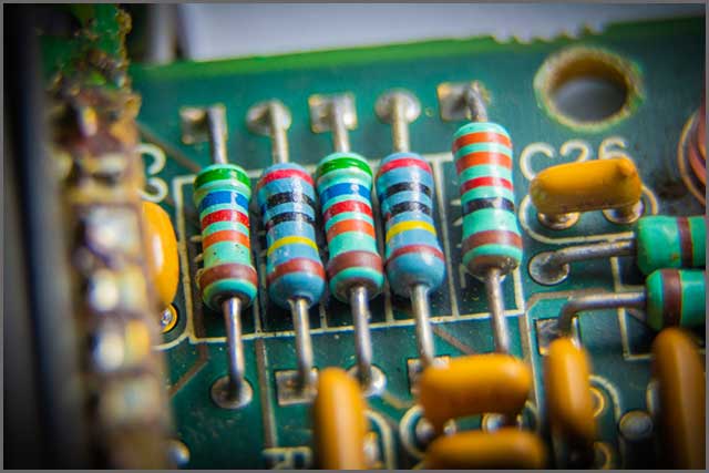 Image 2: Resistors Description
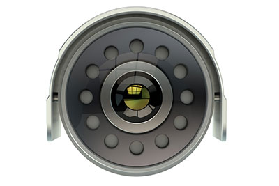
1.2 Integrated circuits
Integrated circuits or ICs are typically dubbed as miniature versions of PCBs. The chips inside the IC themselves are relatively tiny and hard to connect to a PCB directly. However, you can connect an integrated circuit directly to a PCB with ease.
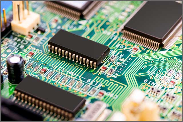 Image 3: IC Description
1.3. Silkscreen
Silkscreen typically refers to the layers of ink traces that you use to mark various components on a PCB. The markings are mainly for identifying and highlighting test points/logos. They are also used for warning symbols. For most PCBs, the silkscreen lies on the component portion. There are some exceptions where you can mount it on the solder side as well.
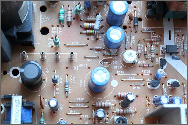 Image 4: Silk Screen Description
1.4 Vias
When it comes to a PCB design, vias or via comprises two pads. You see them laid such that they correspond to one another on different layers on the PCB. You will know that they connect through a hole that is present in the circuit board itself.
1.5 Capacitors
Capacitors are electrical components that store an electric charge. They typically consist of a pair of conductors or, even more, separated in between with an insulator. For PCBs in particular, capacitors are organized to allow the passage of AC but block DC from flowing.
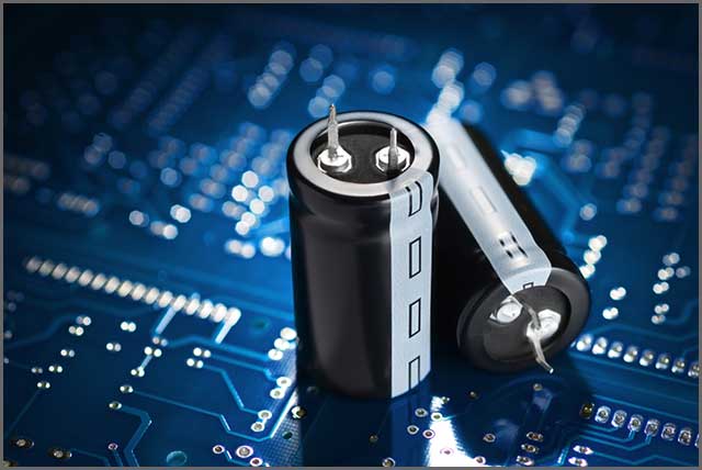 Image 5: Capacitor Description
1.6 Diodes
A Diode is an electrical device that allows current to flow in a single, specified direction. So naturally, it prevents the flow of recent coming from the opposite direction. It consists of two terminals, namely, an anode and a cathode. A diode is commonly dubbed as a 'unilateral semiconductor device.'
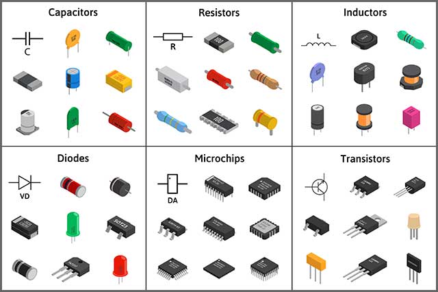 Image 6: Diodes Description
1.7 FR4
FR4 or FR-4 is a material that comprises woven fiberglass along with an epoxy resin binder. It is a relatively cheap material and is available readily in the market. That means that the FR4 is flame resistant.
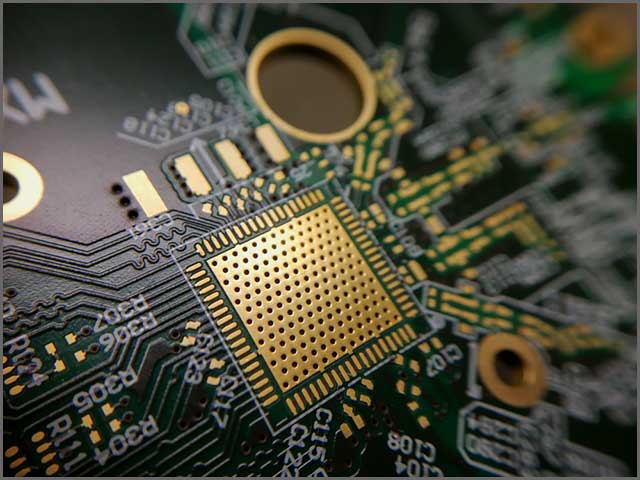 Image 7: Substrate
2、What are the PCB Electronics Characteristics You Can Choose?
2.1 Through Hole
Initially, the through-hole technology was widespread in manufacturing PCB electronics. It was done by embedding the edges through holes that were present on the side of the board. For this process, different electrical components got mounted in place using leads. On the other hand, you saw the components soldered up on copper traces to set them in place.
 Image 8: Through-hole Tech
2.2 Surface Mount
Surface mount technology first appeared in the 60s, but it started making a mark in the 80s. Nowadays, the surface mount is typically preferred for PCBs. It is far more convenient because the electric components can now be soldered directly on the board's surface. That is because the parts have updated designs consisting of smaller ends caps and metal tabs.
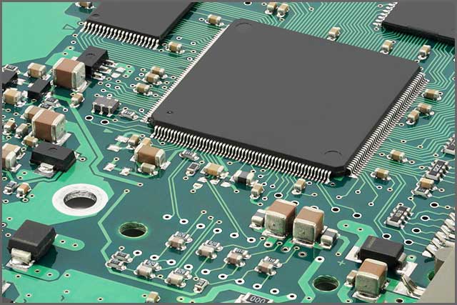 Image 9: Surface Mount Tech
3、What are the Common PCB Electronics Problems?
3.1. What are Plating Voids?
Plating Voids occur when there is a problem with the deposition on the board. Faults in sedimentary affect the structural integrity of the hole walls. It prevents the PCB from functioning correctly. Plating voids can form when there is an uneven coating of Copper. That may occur because of rough drilling, the presence of air bubbles, and contamination.
The best to avoid the formation of Plating Voids is to ensure that the drilling process is smooth. You can do this by following the manufacturer's directions. That includes the speed of the drill and the recommended number of drill hits.
3.2. What problems can arise for not using DFM?
DFM or 'Design for Manufacturability' is an integral aspect of manufacturing PCBs. DFM analysis software can solve design problems before the manufacturing process. It also makes it easier to spot problems in the structure later on if it malfunctions. Without DFM software, it is hard to pinpoint the issues in a PCB. For one, then manufacturers and designers have to work off of intuition or guesswork.
To avoid similar problems, invest in some reputed DFM tools that are available on the market. It is bound to ease the manufacturing process and make it more efficient.
3.3. What is Inadequate Copper to edge clearance?
Copper is a common raw material for manufacturing PCBs. It is highly conductive; however, it is also soft and, therefore, prone to erosion. To prevent corrosion and isolate the Copper, we will cover some other materials instead. However, the problem arises when it is incredibly close to the edge. You will see that it's trim when the PCB is trimmed. That leaves the Copper exposed and causes the PCB to malfunction.
The solution is simple; ensure that there is enough room between the layer of Copper and the edge of the circuit board. This way, it does not run the risk of getting trimmed along with the PCB. You can set specific clearance standards using DFM software as well.
Special Offer: Get $100 off your order!
Please email [email protected] for details.
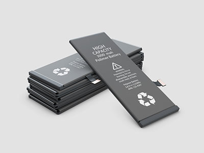
4、Having Silver in PCB Electronics: The Problems
Copper is prone to corrosion owing to its soft texture. It makes the PCB vulnerable to malfunctioning as well. The case with Silver is also relatively similar. You avoid using Silver in PCB electronics to prevent corrosion and preserve the structural integrity of a PCB.
When it comes to designing and manufacturing Electronic components, Gold is merely unparalleled. The attributes of Gold make it an ideal choice, particularly for PCB electronics. Since it is relatively malleable, you can use it for a variety of components. It carries limited amounts of current and is an excellent electric conductor. Gold requires lower resistance and voltage. Therefore, it is much more durable.
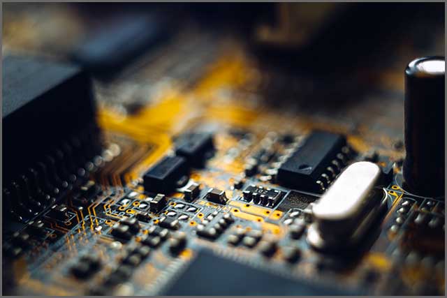 Image 10: Gold For PCB Designs
5、Should you worry about missing solder masks between pads?
It is common knowledge that a PCB is a relatively compact device. Therefore, it is quite common to find that there are no solder masks between pads. It can lead to the formation of solder bridges. It is why we do not recommend that you ensure the presence of solder masks between pads or pins so that your PCB does not cause a malfunction.
6、Why are Acid Traps Worrisome in PCB Electronics?
While manufacturing PCBs, PCB etching is a necessary process. Here, you remove the extra Copper from the PCB electronics. You can use several different acidic materials for this purpose. However, more often than not, this can lead to the formation of acid traps. That is problematic because the acid can corrode the Copper tracing and other components of the PCB, rendering it unusable.
The best way to avoid this is to ensure that traces are not placed at acute angles during the etching process. Also, it is essential to ensure that there is ample distance between the paths and the vias.
7、What Electromagnetic PCB Electronics issues can you face?
Electromagnetic issues occur when there are irregularities in electromagnetic compatibility and interference. Manufacturers and designers have to make PCBs that minimalize the effects of these energy elements.
It is best to increase the ground area of the PCB to reduce noise, cross-talk, and the rate of emission to correct the problem of electromagnetic. Alternatively, you can categorize Electromagnetic Interference by separating the digital and analog components of the circuit.
8、Conclusion
By now, you are aware of basically everything that can go wrong while manufacturing PCB electronics. The list is long enough, so naturally, it makes this last part particularly important. That is, choosing a proper PCB electronics manufacturer. It would help if you took your time with this decision. There are multiple factors to consider.
Talk to us today to know how we can help you with designing customized PCB electronics solutions. You have nothing to worry about with our quality control, efficient design, and good structural integrity/manufacturing. Order PCB electronics that fit your needs prevent surprises later on and end up with a genuinely durable offering.
Special Offer: Get $100 off your order!
Please email [email protected] for details.