Surface-mount technology has become famous for building better assembly yields. Nowadays, the technology aims to make lightweight and more efficient electronic packages. It is essential to use integrated circuits with better electrical properties. An excellent type of surface-mount packaging is the Ball Grid Array.
However, it is essential to note that there are different BGA package types. Let's learn about them. Also, you find things to consider before choosing BGA package sizes, including the advantages and disadvantages.
Contents
- What is the BGA package?
- Advantages and disadvantages of the BGA Package
- Advantages of the BGA Package
- BGA Package Types
- Ceramic BGA (CBGA) Package
- Plastic Laminate BGA (PBGA)
- Tape BGA (TBGA)
- Enhanced ball grid array (EBGA)
- Flip Chip BGA
- Metal ball grid array (MBGA)
- Micro BGA
- BGA Package Sizes
- Another packaging
- Conclusion
What is the BGA package?
BGA or ball grid array is an SMD component without leads. In other words, it is a surface mount technology that fits onto an integrated circuit board. Typically, it has solder balls that pass electricity from the package to the circuit board.
Further, the BGA package balls physically connect to the substrate. This substrate, in turn, links to the die by wire bonding. And using conductive traces, it, therefore, passes electrical signals between the balls and the base.
Advantages and disadvantages of the BGA Package
-
Advantages of the BGA Package
Using solder with the BGA package against the substrate comes with several benefits. However, the most relevant are:
- More compact: The package does not occupy much circuit board space.
- Self-aligning: It has good adhesion properties because of the ball-shaped shoulder joints.
- Less thermally resistant: The solder ball joints allow better heat dissipation.
- More conductive: A lot of small-size joints, thus, means it conducts better electricity.
- Disadvantages of the BGA Package
In the same way, the BGA has a few drawbacks, such as:
- The difficulty of inspection: It is difficult to inspect the molten solder joints and solder balls for flux residue after soldering.
- Difficulties during circuit development: Special equipment requires very careful handling.
- Cost of equipment: Relatively, the BGA package is expensive.
Special Offer: Get $100 off your order!
Please email [email protected] for details.
BGA Package Types
Typically, BGA package types differ according to the substrate material involved. However, there are three main types. They are:
-
Ceramic BGA (CBGA) Package
CBGA is a ball grid array package made of a ceramic substrate. However, there are many different package options in this particular category.
Further, the ceramic ball grid array has an edge in terms of thermal expansion coefficient. Its solder balls comprise 90 percent lead and 10 percent tin. This composition, therefore, makes the BGA more reliable.
-
Plastic Laminate BGA (PBGA)
The plastic ball grid array, a Motorola invention, uses a plastic substrate. Also, its solder balls consist of 63% tin and 37% eutectic lead. However, the substrate materials involved are:
- Polyimides
- Dry clad
- Bismaleimide triazine epoxy glass
Interestingly, PBGA also supports flip-chip designs. Therefore, you have better connectivity between the circuit board and the package.
-
Tape BGA (TBGA)
This package type creates fine lines with a flexible interconnect on its solder balls. In addition, the package design allows the chip and heat sink to face down. So, it is very good for managing heat too. But, if you face the chips down, you should select flip-chip technology. Alternatively, if the chip faces up, you select wire bond.
TBGA is generally excellent for thin packages and applications that need high efficiency. Hence, it is relatively costlier than PBGA.
-
Enhanced ball grid array (EBGA)
This enhanced ball grid array is yet another type of PBGA with an added heat sink for better thermal performance. You establish an electrical connection with the chip facing down on PCB and select the wire bond.
-
Flip Chip BGA
FC-BGA uses BT resin instead of Ceramic as a substrate material. Therefore, it improves electrical performance. It saves cost and helps reduce internal circuit loops.
Further, its tin-to-lead ratio is 63:37. This composition, thus, improves surface tension at the melting state. Therefore, it is easy to adjust the chip positions without a flip-chip alignment tool.
-
Metal ball grid array (MBGA)
The MBGA uses an aluminum substrate. It connects the solder mask and aluminum base using microchip module technology and a thin film. Like the TBGA, there is the metal ball grid array produced by Olin. Overall, MBGA and TBGA have excellent heat and electrical performance.
-
Micro BGA
Produced by Tessera, this package type works with its chips facing down. Also, its substrate uses packaging tape. In addition, there is an elastomer layer that helps ease thermal expansion stress between the tape and chip.
The main positive about the Micro BGA is its tiny size. As a result, it is popular for use in many compact applications. Moreover, it also has fewer pins, mostly suitable for storage devices.
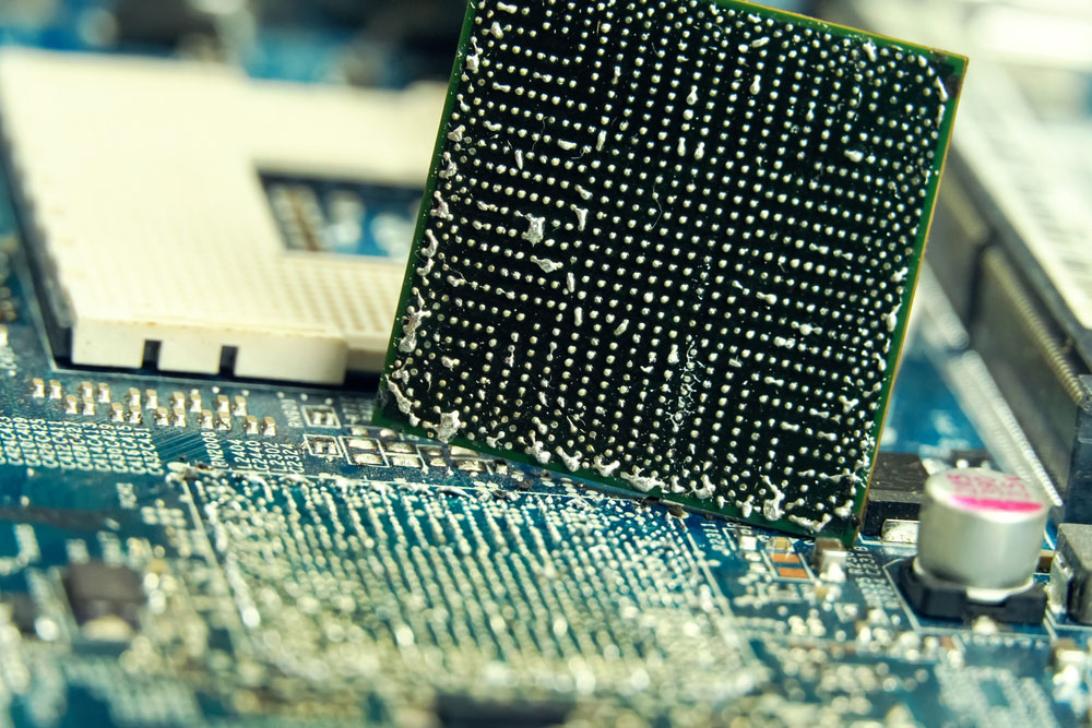
(A ball grid array on PCB).
BGA Package Sizes
PCB designers consider package sizes because of pad size and opening for solder masks. So, generally, pad size is approximately 85% of the BGA ball size.
So, to help you get the best out of your BGA projects, here are some guidelines.
- For BGA PCB designs of 0.4mm pitch, use an NSMD pad size.
- Also, do not reduce BGA pad sizes for ball sizes of 0.5mm pitch or less. Otherwise, there won't be enough space for the soldering process when using a reflow oven.
- Create a bridging between NSMD pads when using ball pitches less than 0.4mm.
- Most pad sizes are small. Therefore, solder mask webbings do not often give enough adhesive strength.
- Ensure to leave no traces between BGA pads on the external layers.
- However, on the internal layers, only one trace is advisable. Anything else leads to PCB fabrication issues.

(The designer is designing the PCB size)
Another packaging
Other packaging types include:
- PoP Package Types
This package is, otherwise, a double-stack design. The lower chip is the CPU, while the top chip uses random access memory. As a result, these packages easily fit into a smaller PCB print.
- LGA Package Types
The land grid array is a package type using solder balls for connecting the package and circuit board. Meanwhile, some LGAs come with pins for those that use sockets.
- QFN Package Type
QFN means quad flat no lead pack. This design is a variation of the QFP package type with no pins. However, the quad flat package is a surface-mounted chip that sends leads from all four sides.
- Flip-Chip
This design of flip-chip has its active side facing downward. And although it permits connections via solder ball joints, its main benefit is reducing distance and inductance.
Conclusion
A ball grid array is a miniature package for surface mount technology. Typically, solder balls in solder connections hold the substrate for wire bonding.
Now you have learned all about BGA package types. However, if you are unsure about the best surface-mount package for your electrical project, contact us for assistance.
Special Offer: Get $100 off your order!
Please email [email protected] for details.