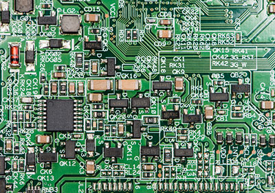
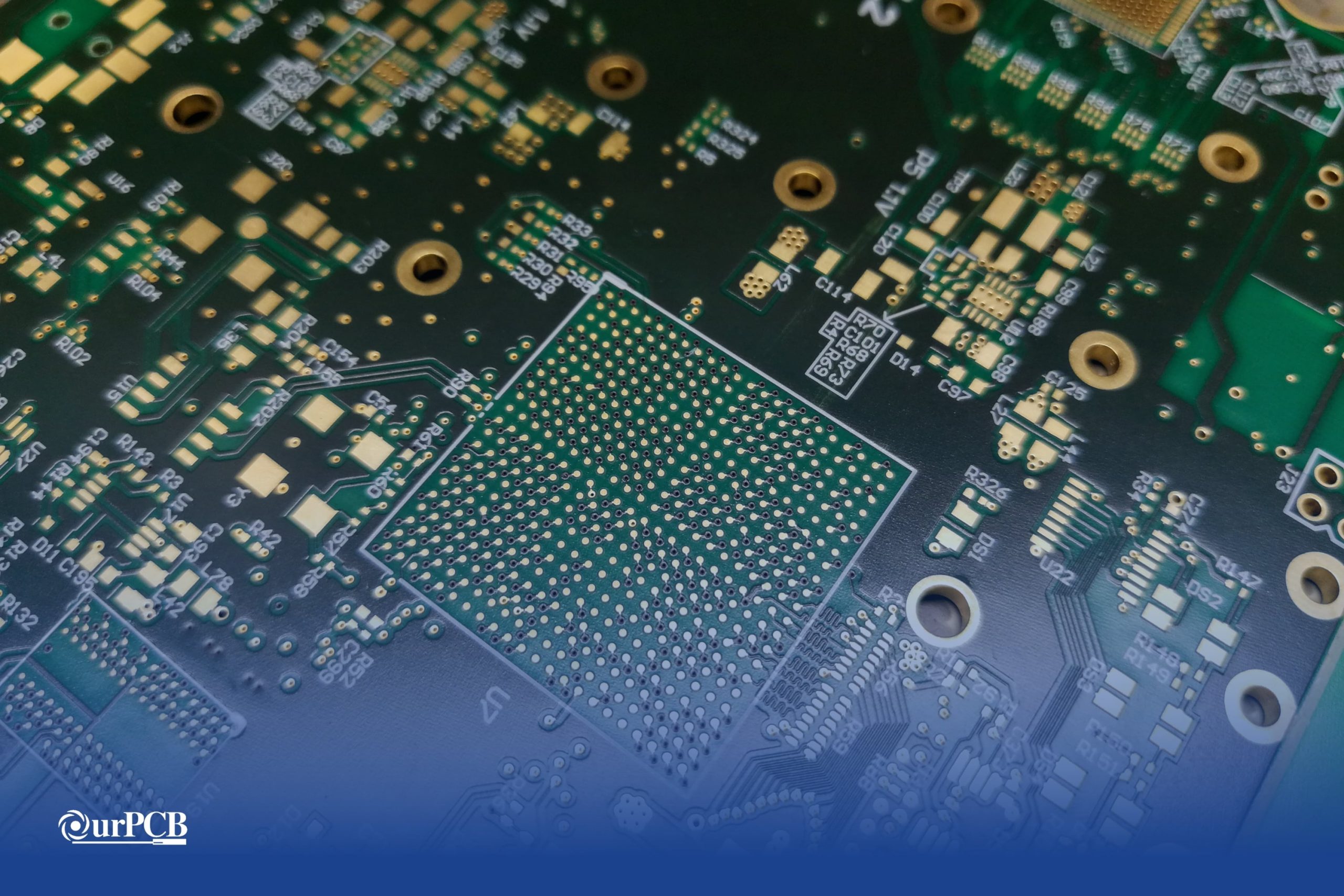
BGA stands for ball grid array and BGA PCBs are surface mount packaging units used for ICs or integrated circuits. Traditional PCBs use pins for connecting circuit boards and the package. However, BGA PCBs use solder balls instead as connecting points. Due to this unique feature, they’re capable of forming high density connections, which are required in modern electronics.
They also offer space efficiency and better heat conduction. BGA PCBs are common in devices that need heat dissipation and power processing such as in computers, smartphones and other modern gadgets.
Contents
- How does a BGA PCB differ from other PCBs?
- Components of a BGA PCB:
- BGA Vs. CGA (Column Grid Array)
- Key Advantages of BGA:
- Excellent for Complex Electronics
- Improved Electrical Performance
- Allow for Smaller, Denser Designs
- Lower Thermal Resistance
- Better Signal Integrity
- More Durable
- What are the Different Types of BGA Packages?
- BGAs Per Use Case
- For Compact Designs
- For Reliability
- For Cost-Effectiveness
- What to consider when choosing a BGA Package
- The BGA Manufacturing Process:
- Substrate Fabrication
- Ball Attachment
- Solder Reflow
- Underfill
- Cleaning
- Inspection and Testing
- What Materials are used in BGA Packages?
- The BGA Assembly Process
- PCB Preparation
- BGA Placement
- Reflow Soldering
- Cooling and Inspection
- Secondary Processes
- What is a BGA PCB? | FAQ
- What Are Some Potential Challenges Of Using BGA PCBs?
- What are Key Considerations for BGA Placement and Routing On a PCB?
- How Many Layers are Needed for BGA PCB Design?
Special Offer: Get $100 off your order!
Please email [email protected] for details.
How does a BGA PCB differ from other PCBs?
BGA PCBs use a grid of solder balls as connection points underside integrated circuits. As a result, these PCBs can form high density connections in a smaller footprint.
Also, the BGA technology is highly intricate and you need specific equipment. Such equipment is capable of handling dense and small BGA packages. Some key equipment that makes the BGA manufacturing complex include die attach machines, substrate fabrication tools, ball placement machines, and wire bonding equipment.
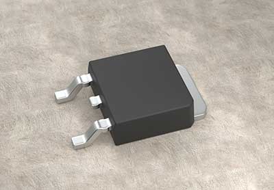
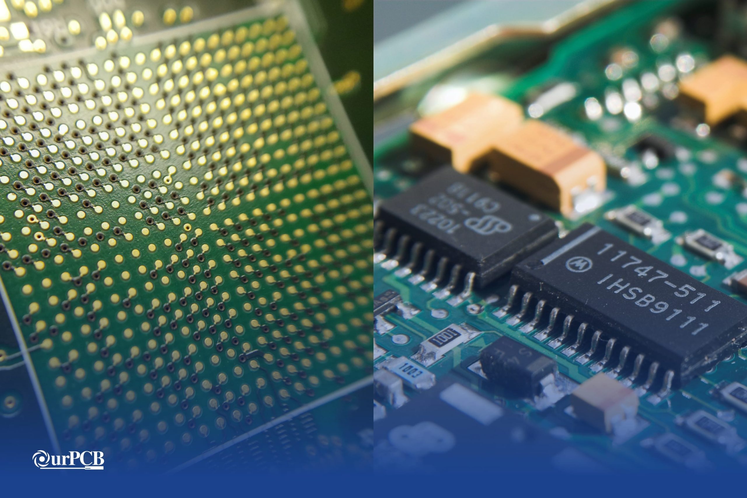
Components of a BGA PCB:
- Ball Grid Array Package: This is the core component of all BGA PCBs. The package has an array of solder balls on its underside.
- PCB Substrate: Made from BT resin or FR4, the substrate layer helps support the IC chip and connect the chip to the solder balls.
- Solder Mask: This is a protective coating applied on copper traces to protect from oxidation. It also prevents solder bridges by directing solder flow to the required places only.
- Solder Balls: These are small balls of solder lying between PCB and IC chip. These are arranged in a grid on the underside of the integrated chip.
- Copper Pads: PCB pads or copper pads align with the solder balls of the BGA package to set electrical connections.
- Traces: These conductive pathways on PCB connect different components electrically including BGA pads, routine signals from one point to another.
- Vias: Vias are small holes drilled in different layers of BGA PCBs. These conductive holes connect traces of different layers in a multilayer PCB and to route BGA pads to the PCB’s internal layers.
BGA Vs. CGA (Column Grid Array)
Both BGA and CGA are meant for mounting integrated circuits but there are considerable differences between the two.
| BGA | CGA | |
| Connections | BGA uses an array of solder balls as connection points. | Column grid arrays use column-shaped interconnections. |
| Features | In BGA, balls of solder melt down to form electrical connections. | In CGA, metal columns have high melting points. As a result, they can withstand high thermal stress ensuring robust connections. |
| Applications | BGA PCBs are best for complex electronics requiring high density connections, better heat dissipation, and improved electrical performance. | CGA is best for applications undergoing extreme thermal stress ensuring high reliability. |
Key Advantages of BGA:
Excellent for Complex Electronics
Today’s complex electronics need high-density interconnections, space-saving configurations, and effective thermal management. Due to BGA’s capability of accommodating a large number of connections in a small space, it’s beneficial for high-end consumer electronics and telecommunication devices.
Improved Electrical Performance
Due to high thermal conductivity and better heat dissipation, the design of BGA PCBs is perfect for high-performing devices like memory chips and microprocessors. These PCBs can handle more heat released from the dense circuit designs. Also, the short connections between the BGA package and the board creates short electrical paths. Shorter connections means low inductance, which means reduced signal distortion and improved signal processing.
Allow for Smaller, Denser Designs
In pin grid arrays, to reduce the size of the board, more and more pins are added. However, it results in soldering issues and increased chances of bridging between adjacent pins. On the contrary, BGA PCBs use a grid of solder balls which can accommodate more interconnections in a small space. Space efficiency of BGA makes them perfect for modern compact devices.
Lower Thermal Resistance
Due to lower thermal resistance of BGA PCBs, heat flows freely and easily, preventing overheating of devices. The use of thermal balls, the metal core design, and use of materials with high thermal conductivity, all contributes to the lower thermal resistance of these PCBs.
Better Signal Integrity
Maintaining better signal integrity means lesser distortion of signals. Due to shorter electrical paths, BGA PCBs have lower inductance, leading to smooth signal processing with minimal signal distortion even in high-speed circuits.
More Durable
In pin grid arrays, the long pins are prone to bend and break. However, the solder balls in BGA PCBs ensure string solder joints. Further, the BGA grid distributes the mechanical stress evenly to a large number of solder balls, making them less susceptible to physical damage.
Special Offer: Get $100 off your order!
Please email [email protected] for details.
What are the Different Types of BGA Packages?
- PBGA: Plastic Ball Grid arrays or PBGA uses plastics as its packaging material and glass laminate or BT resins as the substrate. The PBGA uses lead and lead-free solder balls and you don’t need to use extra solder for creating connections to the package and the solder balls. Its structure is quite innovative, making it possible to create high-density interconnections. It ensures optimal thermal management but is sensitive to humidity. This BGA type is quite popular due to its cost-effectiveness.
- CBGA: CBGA stands for Ceramic Ball Grid arrays. As a substrate, it has multiple layers of ceramic with a metal cover to ensure chip protection. The balls are made from high-temperature eutectic material and due to this, it has unmatched thermal stability. For devices requiring high temperature flexibility, CBGA is an exceptional performer. The only disadvantage is its high cost.
- TBGA: TBGA stands for Tape Ball Grid array and this BGA variety is a perfect combination of performance and flexibility. This structure has a hollow cavity, making it flexible for innovative designs. The interconnections between package and chip are of two types: inverted solder bonding and lead bonding. Due to its excellent thermal management, its heat dissipating properties are incomparable. Its sleek structure makes it perfect for use in portable devices. Among all BGA varieties, this is the most cost effective one.
- Other BGA varieties:
- Micro Ball Grid arrays: miniature varieties offering high-density interconnections in a very small area.
- LGA package types (Land Grid Array): these have lands or pads in place of solder balls.
- POP package type (package on package): stacks multiple BGAs one on another.
- Flip-chip: does not use wire bonding and attaches the die to the substrate directly.
- Quad Flat no-leads package types: these have uncovered pads on the undersurface.
BGAs Per Use Case
For Compact Designs
Micro BGAs can accommodate high-density connections in a small area. Their compact and intricate nature make them perfect for compact devices.
For Reliability
Due to use of temperature efficient solder balls in ceramic BGA, they offer unmatched thermal stability. Their low thermal resistance ensures high heat dissipation, making it highly reliable for military, aerospace and other such industries.
For Cost-Effectiveness
Plastic BGA uses plastic as packaging material, which costs much less than ceramic material. Also, the manufacturing process is quite simple, reducing the production costs. If you’re looking for cost-effective BGA options, go for plastic BGAs.
What to consider when choosing a BGA Package
You need to consider several things when choosing a BGA package. This is important to make sure you pick the most suitable package for your intended application.
- Package Size
First, make sure the package size is compatible with the circuit board area and the integration you need.
- Number of Pins Needed
The number of pins in a BGA determines the number of electrical connections it can set between integrated circuit and PCB. For complex and high-density connections, you may need a BGA with a high number of pins, while for simple electric connections, fewer pins will work.
- Thermal Capabilities
To ensure performance and reliability of any device, it’s essential to consider thermal performance of the BGA package. BGA packages with low thermal resistance offer better heat dissipation, making them more reliable.
- Costs
The cost of different BGA packages is quite variable due to differences in materials and thermal properties. You need to consider the cost of the package and make sure it aligns with your project budget.
- Intended Application
You may use BGA packages in different products with different lifecycles and working environments. Choose a BGA that can offer reliability and robustness for the working conditions of the intended application.
The BGA Manufacturing Process:
You need to follow several steps to create a high-quality BGA PCB. These include:

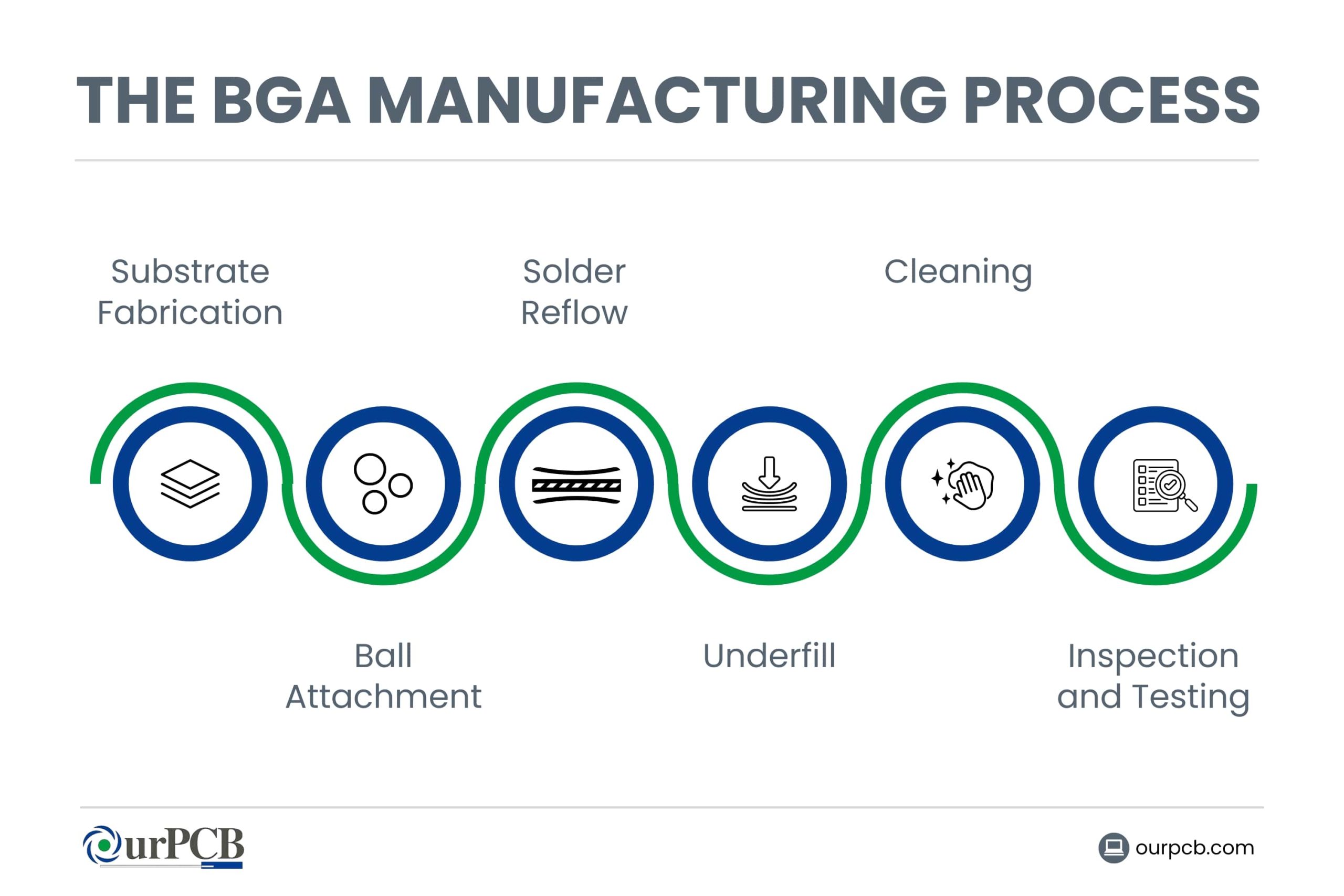
Substrate Fabrication
The substrate is essential for mechanical support. It mainly comprises FR4 material with a copper lamination. Next, you need to attach the IC die to the substrate after cleaning it. For attachment, you may need a conductive adhesive. Once you attach the IC die and substrate, you may need to set wire bonds between them using gold or aluminum wires.
Ball Attachment
This step involves policing the solder balls on the underside of the substrate in a grid array.
Solder Reflow
Next, the BGA package with solder balls is ready to be placed on the PCB. You have to treat the PCB with a solder paste before placing the BGA package. Then the whole assembly is put into a reflow oven, where the solder melts to create strong bonds between the package and the board.
Underfill
This is an optional step and involves injecting an epoxy resin beneath the BGA package. Underfilling is suitable for applications that need better thermal conductivity.
Cleaning
Cleaning may use solvent-based or water-based methods to remove flux residues. Removal of flux residues and any other contaminants is essential for improved electrical performance and solderability.
Inspection and Testing
Once the reflow process is complete, it’s time for inspection and testing. Carefully observe any misalignment or poor joints visually. Several other testing methods are available including electrical testing, x-ray inspection to check functionality of the BGA PCB assembly.
What Materials are used in BGA Packages?
Different BGA packages may use different types of materials to create a design to improve heat dissipating, electrical connections, and mechanical stability. These materials are chosen to provide a balance between performance, reliability, and cost. They may include:
Substrate
- PBGA (Plastic): BT resin/glass laminate
- CBGA (ceramic): Multilayer ceramic
- TBGA (tape): polyimide film: excellent thermal stability
Solder Balls:
- Leaded: made of tin-lead alloy, low melting point for easy soldering, smooth joints, less heat-related issues.
- Lead-free: various alloys, often tin-silver-copper combinations. Safe because of absence of lead, corrosion resistance, meets environmental regulations, higher cost.
Packaging:
- PBGA: use glass laminate as base and plastic as packaging material, sufficient heat dissipation, cost-effective.
- CBGA: Metal lid (often kovar) for EMI protection, use polyimide substrate that enhances electrical conductivity, better heat dissipation, robust physical properties.
Interconnections:
- Copper traces: excellent electrical conductivity, cost-effective, easily solderable.
- Gold plating (for contact pads): high resistance to corrosion, good conductor, durable.
The BGA Assembly Process
The BGA PCB assembly process is very intricate. Follow these steps carefully to ensure reliable attachment of BGA packages onto the printed circuit boards.

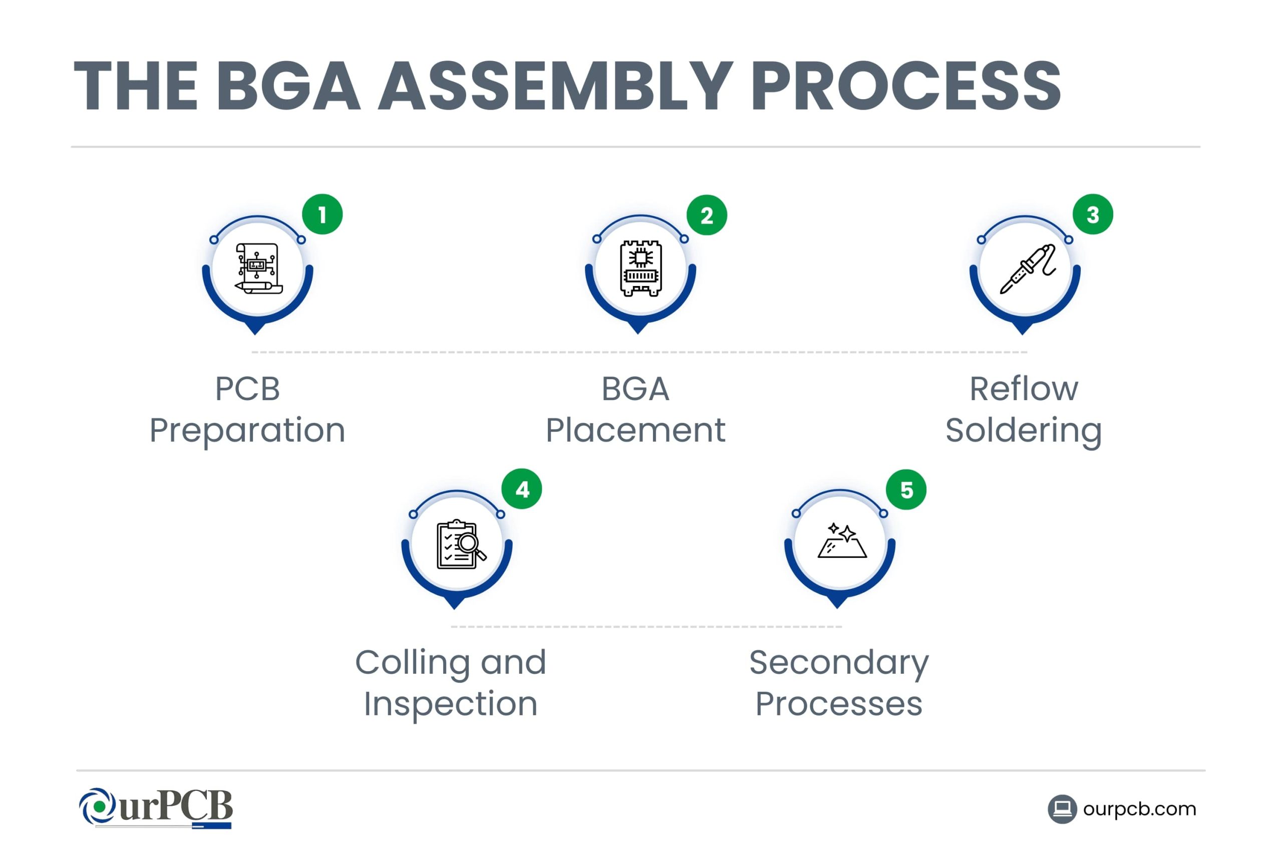
PCB Preparation
Clean the PCB and apply the solder paste on it using a stencil. Make sure that you apply the paste only on the pads where you will mount the BGA.
BGA Placement
Carefully place the BGA package on the designated pads of the PCB. This step requires high precision. Often, high-performing automatic pick-and-place machines are used to complete this process with extreme accuracy.
Reflow Soldering
The BGA is placed into a reflow oven to create strong bonds between the package and the board.
Cooling and Inspection
Once out of the oven, let the assembly cool for some time. When it’s cool, examine the assembly visually for defects and poor joints. You should also do electrical testing to avoid any open or short circuits.
Secondary Processes
After the primary steps, you may need to perform other processes, like testing the assembly for functionality, reworking without damaging components, cleaning or underfilling. Some manufacturers also do conformal coating—applying thin polymer film on circuit boards to protect them from environmental stressors.
What is a BGA PCB? | FAQ
What Are Some Potential Challenges Of Using BGA PCBs?
While using BGA PCBs, challenges may include difficulty in inspection and reworking due to the grid of round solder balls underneath the package. These solder joints are quite hidden, making it difficult to check solder quality and performing any repairs. This greatly affects the reliability of the assembly.
What are Key Considerations for BGA Placement and Routing On a PCB?
For effective implementation of BGA placement, consider the following:
- Signal Routing: to maintain and enhance the signal integrity, make sure you place BGAs to have minimum trace lengths. This becomes more critical for high-speed signals. Also, place the BGA far from the circuit board edge to avoid any mechanical stress.
- Thermal Management: as BGAs generate heat, consider heat dissipation needs. Place BGA while ensuring enough space for thermal vias or heatsinks.
- Component Accessibility: Don’t place components directly under the BGA. Leave at least 200mm space around BGA for easy inspection, testing, and reworking.
For effective implementation of BGA routing, consider the following:
- Escape Routing: Make sure to design appropriate escape routing for signals from the BGA footprint. You may need to consider BGA pitch and the number of layers. It may also involve using vias to route traces away from BGA.
- Trace Widths and Spacing: Stick to proper trace widths and pacing to ensure signal integrity and control impedance.
- Power and Ground Planes: For effective power distribution and return paths, using solid power and ground planes under BGA ensures signal integrity.
- Manufacturing Constraints: Be careful while designing via types, adp sizes and routing density so that your PCB manufacturer can meet your demands and expectations.
How Many Layers are Needed for BGA PCB Design?
For any BGA PCB design, the number of layers you need depends on the number of input/output pins, design complexity, and the specific circuit requirements.
For simple designs and BGAs with low pin count, 2-layer PCBs are enough. Four-layer BGA PCBs are the most common, while 6-layer can route signals without any interference.
Basically, the layers required in a BGA PCB design depends on the project requirements. For further clarifications and to make sure your PCB meets your exact needs, consult with your PCB manufacturer.
Back to top: What is a Ball Grid Array (BGA) in PCB?
Special Offer: Get $100 off your order!
Please email [email protected] for details.