As electronic devices become smaller and their circuit boards more compact, component soldering is getting more complex. This complexity brings about several issues and imperfections in the assembled board. One typical issue that arises when attaching these components is the solder bridge. Let's take a closer look at what a solder bridge is, its causes, prevention measures, and fixes.
Contents
- What is a Solder Bridge on a PCB?
- Solder Bridging Causes
- Commonly Known Soldering Bridging Issues
- Non-Wetting and Dewetting
- Blow Holes and Pin Holes
- Lifted Pads
- Tombstone
- Excess Solder
- What Can You Do To Prevent Solder Bridges?
- Double Check your Circuit Board Design
- Change the Reflow Profile
- Leave a Solder Mask Dam Between Pads
- Use Correct Lead Lengths for Through Hole Components
- Minimize the Solder Paste Volume
- Use Solder Mask Defined Pads for Tight Areas
- Use the Correct Hole Size and Pad Diameter
- Apply Solder Masking Correctly
- Use Fiducials on your PCB
- Work with a Reputable PCB Manufacturer
- How to Fix Solder Bridges
- Monitor the Temperature
- Utilize Surface Tension
- Use the Solder Wick
- FAQ
- What is a Solder Bridge Jumper?
- How to Bridge Solder Pads?
- Summary
Special Offer: Get $100 off your order!
Please email [email protected] for details.
What is a Solder Bridge on a PCB?
A bridge connects two points. In circuit boards, a solder bridge occurs when excess solder connects two or more pads that should be separate above the solder mask. This issue creates electrical shorts that can cause different kinds of damage, depending on the functions of the bridged points.
Solder Bridging Causes
Several conditions can cause solder bridging. They include flawed designs, incorrect manufacturing processes, or faulty equipment. The most typical causes are:
- Using excessive solder on SMT pads due to incorrect stencil specification
- Faulty seals between the bare board and stencil during the printing process
- Relatively large solder pad designs compared to the gap between pads
- Inaccurate component placement
- Tiny component lead size relative to the pad size
- Inadequate solder resistance layers between the pads
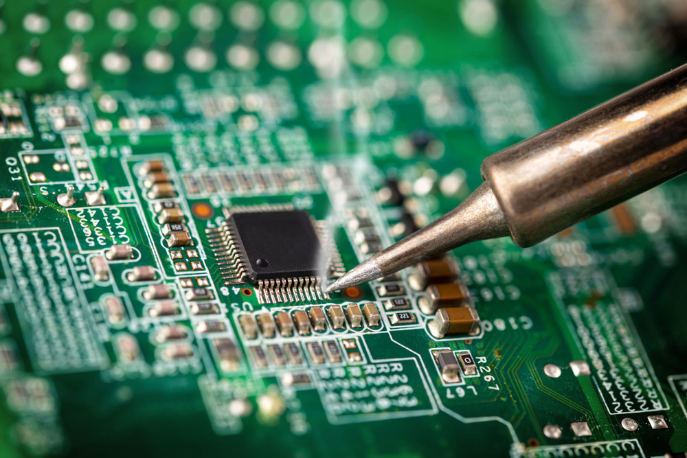
SMD chip solder pads
It is vital to note that liquid solder wicks towards the melted solder or heated metal (a big part of the PCB assembly process relies on this factor). This phenomenon occurs because reflowing solder has high surface tension, so it usually stays balled up where it should be while holding things in it. Anything that interrupts its natural behavior can cause bridging.
Special Offer: Get $100 off your order!
Please email [email protected] for details.
Commonly Known Soldering Bridging Issues
Solder bridging can cause the following problems.
Non-Wetting and Dewetting
Non-wetting refers to molten solder leaving exposed copper behind on the pad. This issue usually happens if brass components haven't received adequate plating or because the flux requires changing.
On the other hand, de-wetting implies molten solder leaves a solder mound on a pad after covering it, then retreating.
Blow Holes and Pin Holes
Both these holes appear when there is poor copper plating or excess moisture on the board.
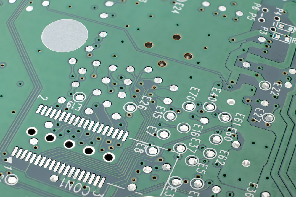
Tiny blow/pin holes on a PCB’s underside
Lifted Pads
Lifted pads can appear when removing a soldered component from an overworked soldering surface joint or one with an uneven copper plating layer.
Tombstone
The tombstone issue occurs when a component gets lifted during wave soldering, making it resemble a tombstone. Using parts with different solderability requirements or an incorrect lead length can cause component lifting.
Excess Solder
Excessive solder accumulation can occur due to an incorrect lead size to pad ratio. Also, it could be due to quick movement on the conveyor belt.
What Can You Do To Prevent Solder Bridges?
Although it is impossible to guarantee the non-occurrence of solder bridges, you can prevent the issue by implementing these preventive measures.
Double Check your Circuit Board Design
Ensure the board design meets the highest producibility levels for both through-hole and surface mount components. You can consult the IPC industry standards for PCB design and assembly, which define level A as the preferred general producibility level. Generally, the best practice is to avoid tiny parts or spacings.
Besides that, check your mask relief design rules for the areas that don't need solder mask application. We recommend setting a relief between 0.003 and 0.008 inches for SMT components. But you might have to adjust this value if the pads are too close together. Also, the solder mask color influences the relief, as shown below.
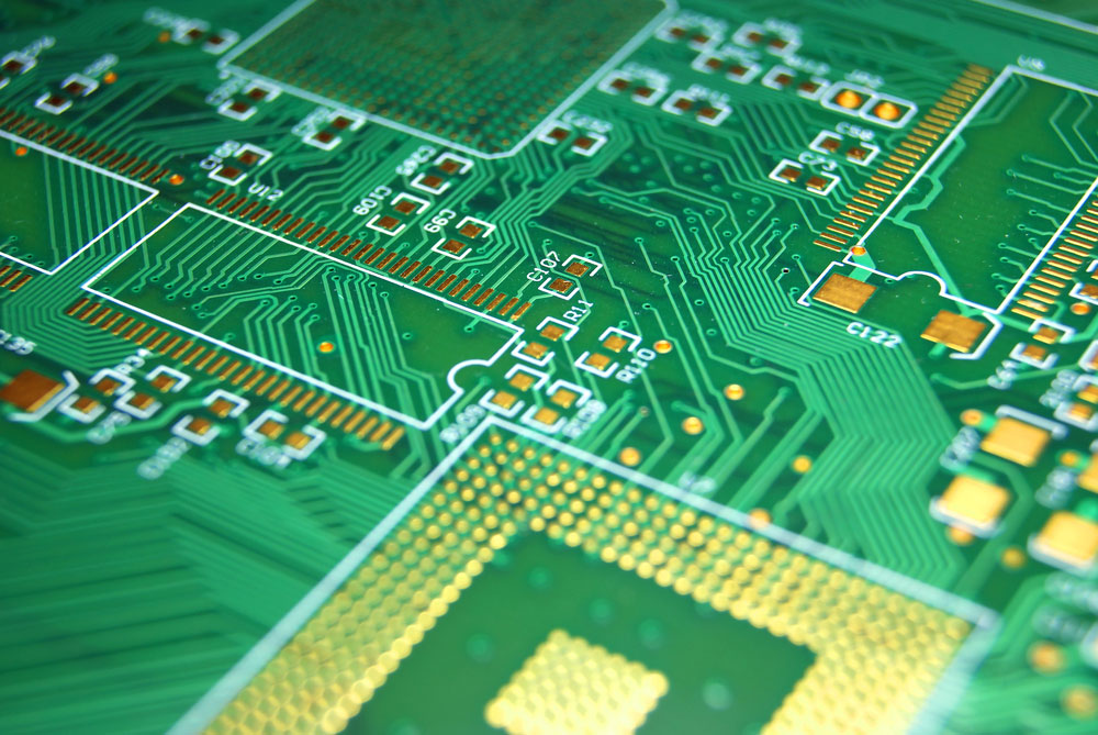
Green solder mask on a circuit board
Change the Reflow Profile
Increasing the period above the liquid solder will give it sufficient time to heat the pads and the component leads to the same temperature. Once at the same temperature, the solder will wet both and move to the required location.
Leave a Solder Mask Dam Between Pads
A solder mask dam is essential between SMT pads because it acts as an isolation wall, preventing spillovers. Generally, the minimum dam size should be 0.004 inches.
Use Correct Lead Lengths for Through Hole Components
The correct lead length depends on the board's size & thickness, component mass & size, and type of soldering. Long leads can cause bridging, and the PCB manufacturer should help you determine the precise length for the application.
Through-hole component leads extending out of a PCB
Minimize the Solder Paste Volume
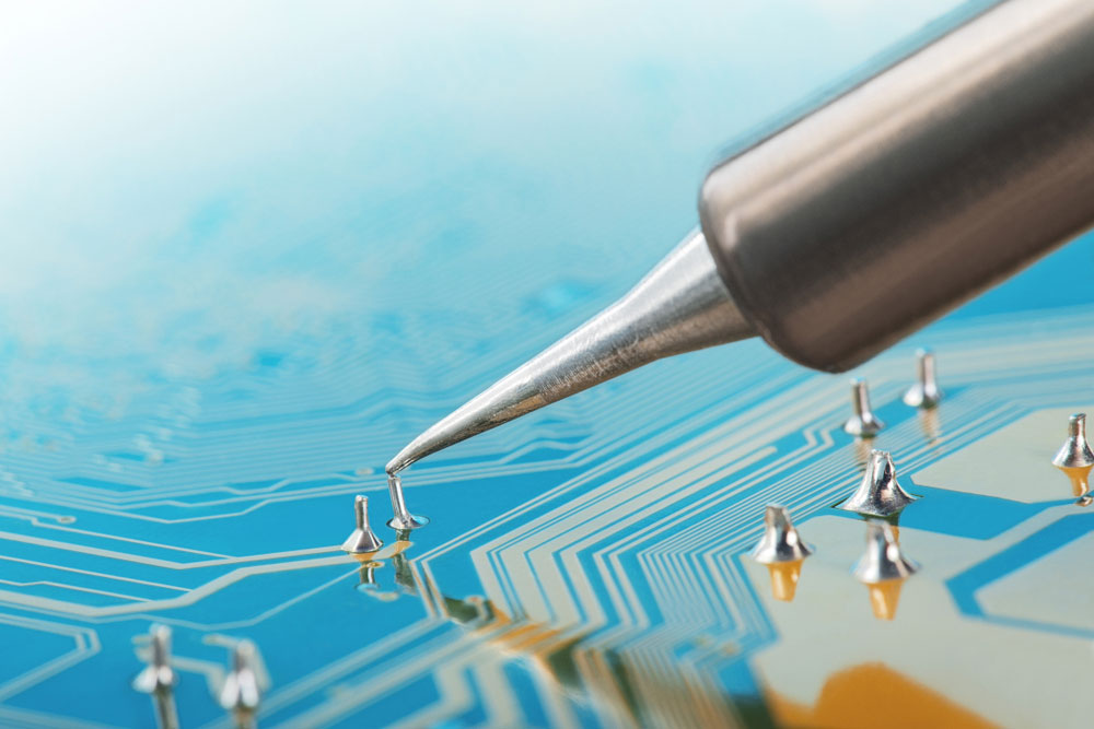
Excessive solder paste application is one of the causes of solder bridges. Therefore, reducing the solder paste volume or modifying the stencil to adjust the application location can minimize bridging significantly.
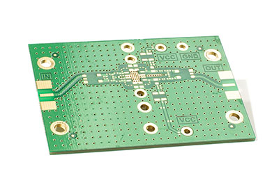
A laser-cut stainless steel stencil
Use Solder Mask Defined Pads for Tight Areas
If there's not enough room for a mask relief and barrier, and you don't need a solder mask dam, you can opt for a solder-mask-defined pad to protect the soldering surface. Ensure you leave a note in the board layout design files to inform the manufacturer about this feature.
Use the Correct Hole Size and Pad Diameter
Large through holes or copper pads decrease the spacing between adjacent soldering surfaces, which increases the chances of solder bridge occurrence.
Apply Solder Masking Correctly
A solder mask is the PCBs top coat applied on all spots that don't require soldering. The typical mask material is epoxy, and molten solder does not adhere to it. Therefore, you should apply the mask between component pins to prevent the solder from sticking there and forming a bridge.
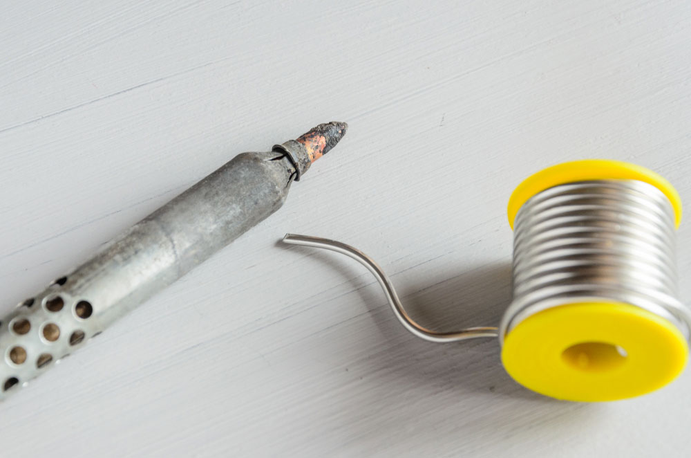
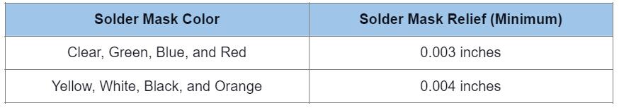
A solder wire and soldering iron
Use Fiducials on your PCB
Fiducials are markers on the PCB design that allows automated machines to locate the PCB, align it correctly, and place components accurately. Misplaced parts increase the chances of solder bridges, and these marks help eliminate this issue. Use at least three fiducial marks on three corners (two on opposite sides).
Work with a Reputable PCB Manufacturer
After sending the design files to the manufacturer, you won't have control over the fabrication and assembly processes. Therefore, you should pick a high-quality and reputable assembly house, and OurPCB is your go-to solution for making solder-bridge-free circuit boards for your project.
How to Fix Solder Bridges
You should have a solder wick, solder flask, and a heat-adjustable soldering iron to fix a solder bridge. With these components, use the following steps to eliminate this issue.
Monitor the Temperature
The soldering iron's tip should transfer enough heat to the solder wick to melt and absorb the solder. Therefore, you need to monitor the temperature and ensure it exceeds the soldering temperature by a few degrees. For instance, if you solder at 250°C, raise the temperature to 270°C. This higher temperature should compensate for the wick's heat absorption from the solder joint.
A soldering iron’s tip
Utilize Surface Tension
You can use the molten solder's surface tension to remove the bridge without requiring a wick. Use a soldering iron with a clean top but be careful not to damage the pads or ICs due to extreme pin/pad heating.
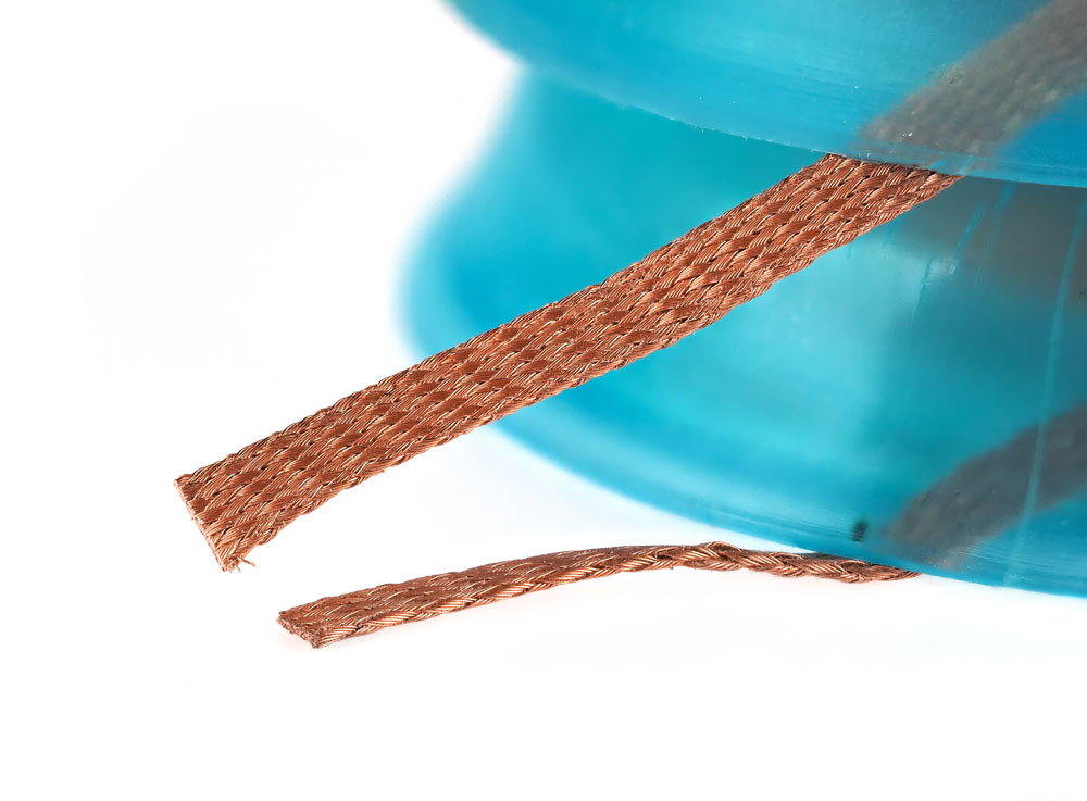
Solder wick
Use the Solder Wick
We recommend using the solder wick to absorb the melted bridge. Apply solder flux, place the wick over the bridge, then heat carefully using the iron. Press the iron lightly over the wick to transfer the heat. Remember to change the wick if it gets filled.
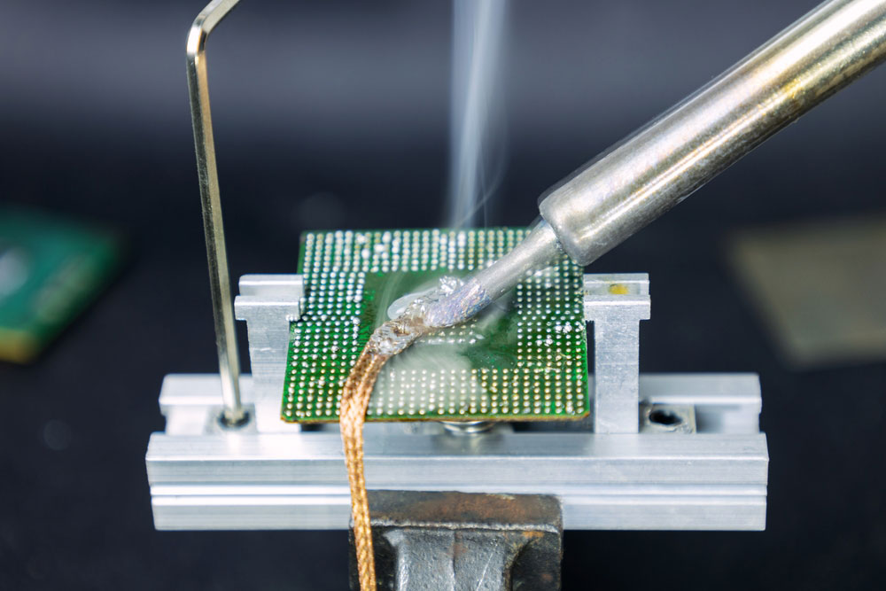
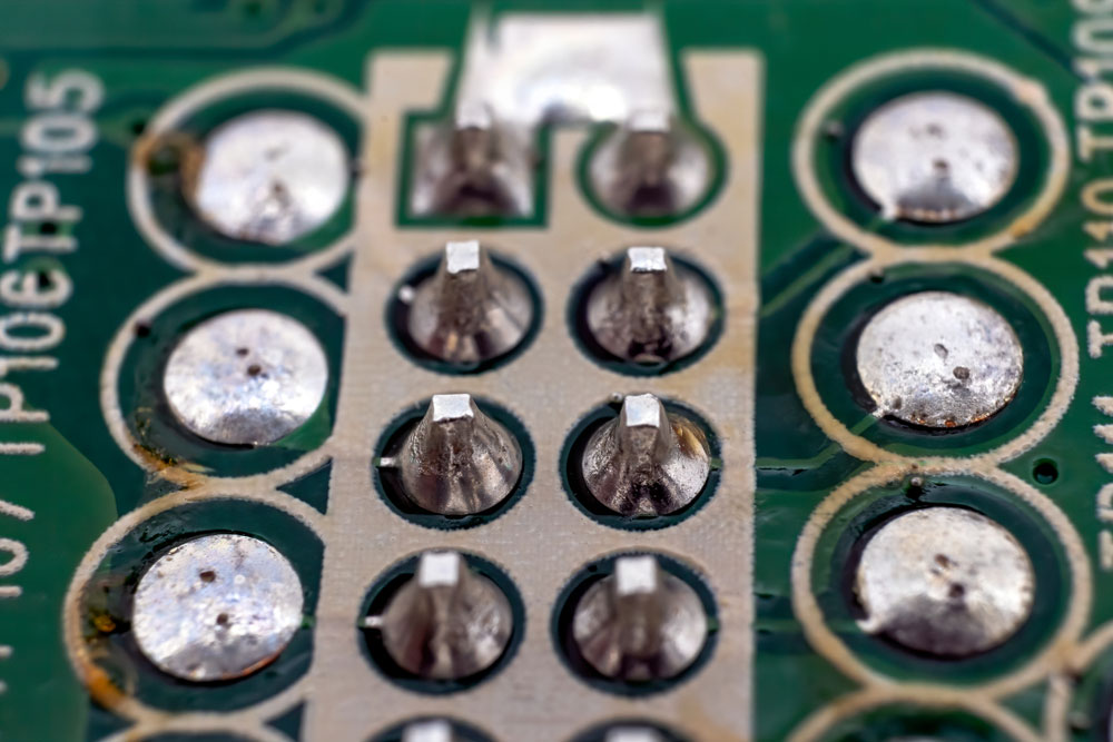
A soldering iron and solder wick removing excess solder from a computer processor
Please note that it is vital to avoid overheating the components or PCB. Also, removing the bridge might remove the solder joint and if this happens, apply more flux and solder the part cleanly back to the board.
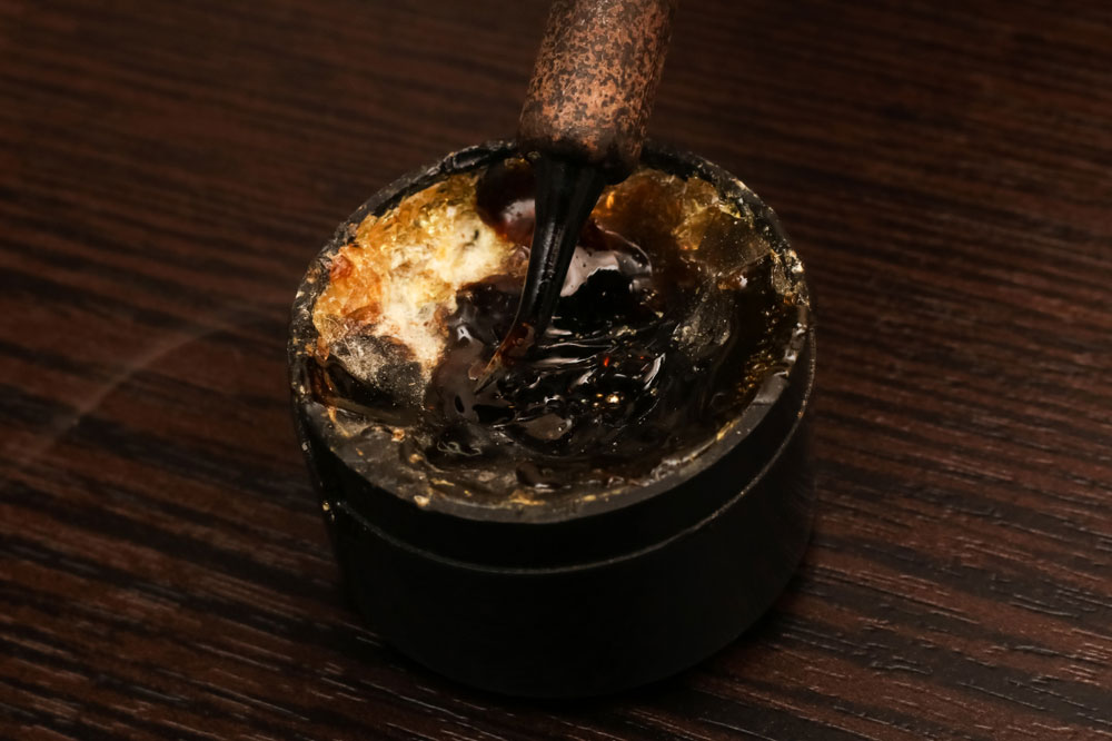
A soldering iron tip dipped in solder flux
FAQ
What is a Solder Bridge Jumper?
A solder bridge jumper is a pair of pads on a circuit board's trace that can get bridged using a solder ball. You can also use a 0-ohm resistor to build the bridge. However, some bridges do not need soldering/joining and should remain open for different applications.
How to Bridge Solder Pads?
As stated above, you can bridge solder pads using a solder ball or a 0-ohm resistor.
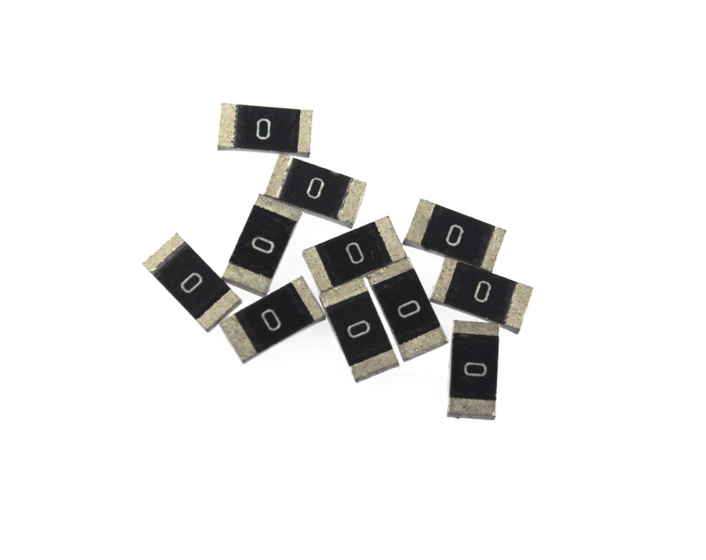
SMD 0 ohm resistor
Summary
In conclusion, solder bridges can be destructive to circuit boards due to shorting, and you should implement preventive measures above to avoid them. However, if they occur, it is possible to do a quick fix. If you want fault-free circuit boards for your project, contact us with your design files to get started on the manufacturing and assembly processes.
Special Offer: Get $100 off your order!
Please email [email protected] for details.