Circuit boards can be incredibly complex but pack the entire circuitry in a small package. So errors can happen during fabrication leading to incomplete electrical pathways that can be expensive to repair later. PCB test points enable manual or automated continuity testing in the early stages of production to identify and rectify problems early on. We will look at these diagnosis points and explain the factors you should consider when designing them. Take a look!
Contents
- What are Test Points?
- PCB Test Point Creation Process
- PCB Test Point Types
- PCB Test Point Systems
- Advantages of Including Test Points
- Which Signals Should Have Test Points?
- Factors to Consider When Designing Test Points on PCBs
- Board Side
- Test Point Distribution
- Board Manufacturing Process Tolerance
- Minimum Test Point Distance
- Zone for Tall Components
- Test Point Shape and Size
- Test Point to Component Clearance
- Test Point to Board Edge Clearance
- Probe Point Identification
- Probe Point Parameters
- Wrap Up
What are Test Points?
PCB test pins or points are tiny wire loops on a circuit board with exposed metal to enable you to inject test signals during production to monitor the electronic circuit. This signal injection helps you test whether the PCB meets its specifications and qualifies for soldering. Most basic PCB designs have these test points on the bottom side, but dense or complex boards can have them on either or both sides.
PCB Test Point Creation Process
A PCB test point must be an exposed metal loop or pad on a circuit board's outer layer that connects to a net. The exposure allows probe tests from the automated test equipment.
Once this is clear, the next step is to flag the required test point locations in the CAD software. The application should go through all these points and select the test point candidates that conform to the requirements set up in the parameters, such as spacing.
After selecting all the candidates, the design software is ready to export the data to the test point file and awaits your command.
PCB Test Point Types
There are two types of test points.
- Soldered Test Points: This type allows for testing and error checking using handheld equipment and has posts soldered on them for test lead editing.
- Automated Test Points: As the name suggests, ATPs allow testing using automated test equipment. They can be metal landing pads, pins, or thru-hole vias.
Special Offer: Get $100 off your order!
Please email [email protected] for details.
PCB Test Point Systems
Three primary systems use these test points on the PCB. They include the following.
- In-Circuit Test (ICT): This test gets done after board assembly. The board goes into the ICT fixture, which has multiple probe devices for every net.
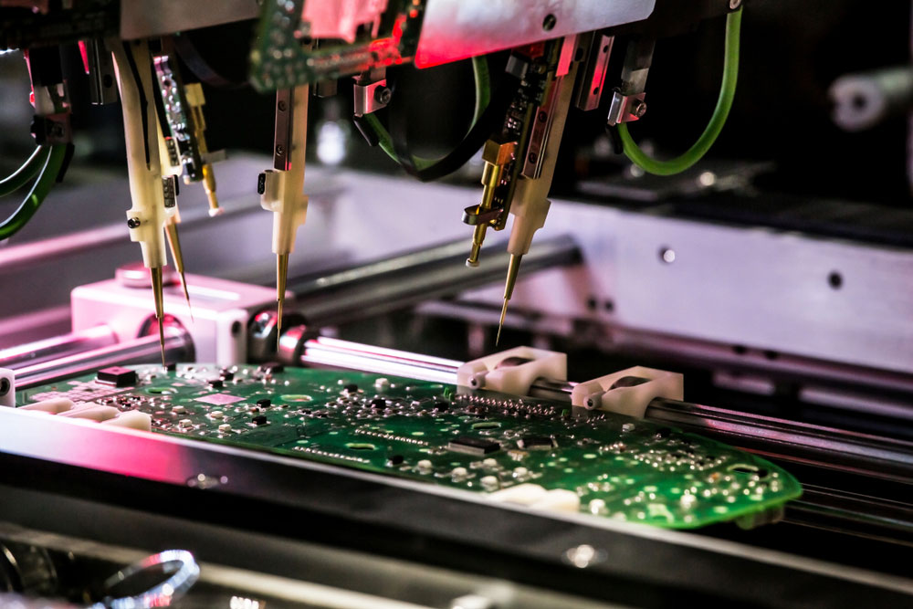
- Flying Probe: The flying probe test also occurs after circuit board assembly on each net by connecting to the test points.
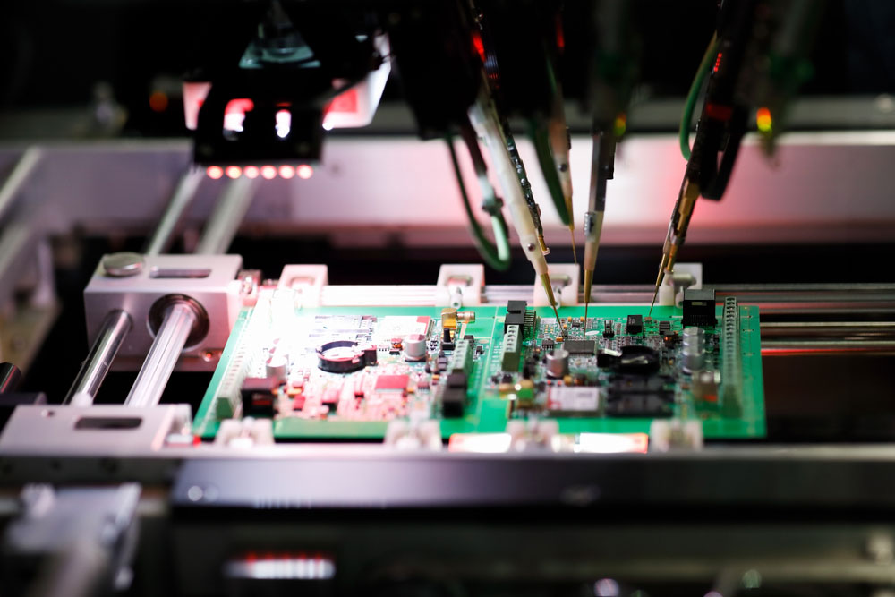
A printed circuit board assembly undergoing a flying probe in-circuit test in a flying probe tester
- Bare Board Testing: As the name suggests, this test occurs after board fabrication and checks if the nets have electrical connectivity.
Advantages of Including Test Points
- Easier and faster error detection: These pins simplify probe testing and enable you to get the test measurements without compromising PCB integrity.
- Cost and time savings: Test points help you detect connectivity issues in the design phase, saving time and money. Without this early testing, you might have to do costlier assemblies later and waste time doing repeat tests on the advanced PCB model.
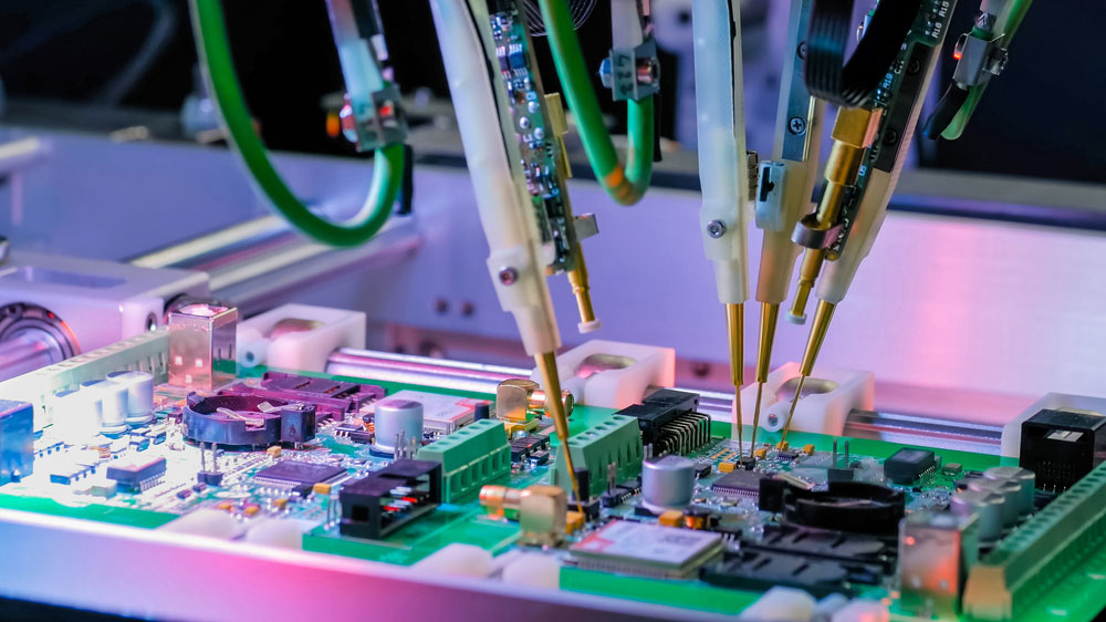
- Low profile: Test points have a significantly lower profile than other test probe point types like turrets and posts. The height of test points is similar to that of surface-mounted components.
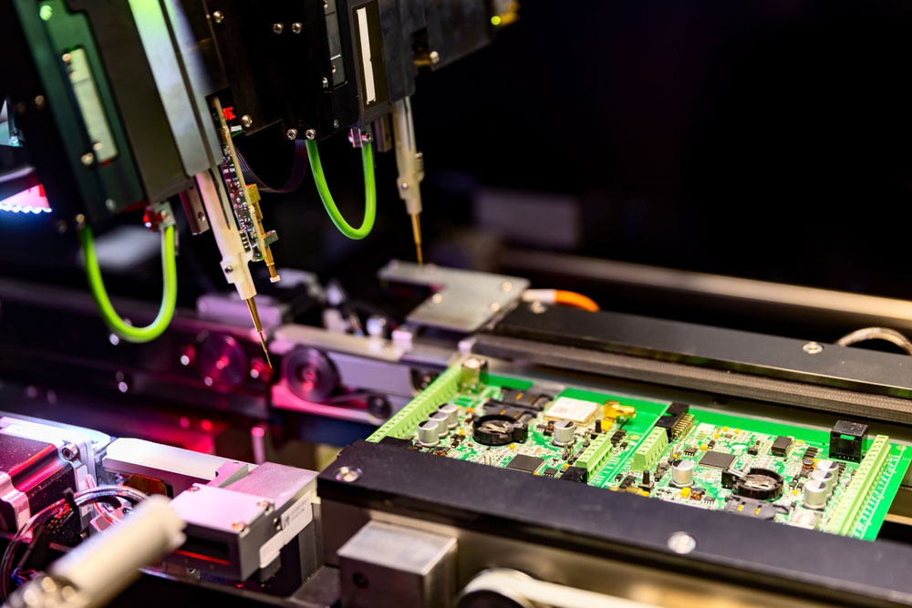
Circuit board assembly and automatic robotic flying test probes in a testing machine. Note the non-noticeable low-profile test points on the PCB.
Which Signals Should Have Test Points?
- Ground
- Power supply
- Programming links
- Serial communication buses
- JTAG ports
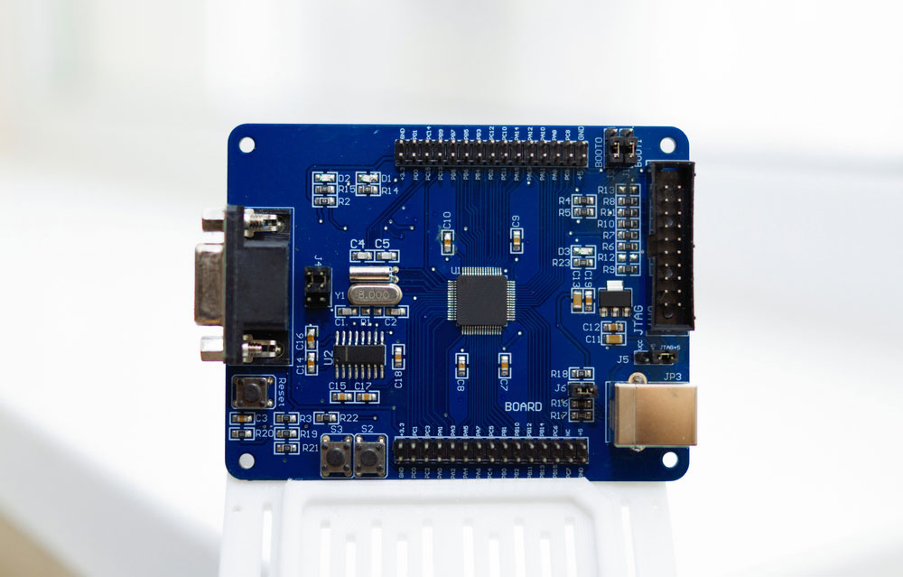
A blue dev board with a JTAG connector
- UART port
- Reset line
- Interrupt line
- Programmable references
Factors to Consider When Designing Test Points on PCBs
Recommendations and factors to consider for correct test point positioning and placement.
Board Side
Usually, placing the test points on one side of the circuit board is more economical on time and money because it streamlines the testing function.
Test Point Distribution
You can test the board using multiple probes if you distribute the test points uniformly, so avoid creating high-density probing areas. Also, placing several test points in one location can exert uneven pressure on the board, which can flex and break solder joints.
A multi-purpose flying probe system testing a PCB
Besides that, keep these points away from obstructions like mounting hardware, overhanging component features, solder masks, etc. And position these points using high-speed design rules to avoid creating antennas that radiate interference.
Board Manufacturing Process Tolerance
Consider the manufacturing tolerances as you build the initial PCB layout. Remember, the board needs enough space to hold the test points and probes when testing.
Minimum Test Point Distance
Two circuit board test points should have 0.1 inches minimum spacing between their centers to enhance testing effectiveness. The broader the distance between these points, the easier it will be to build, change, and maintain them. Also, wider spacing allows you to use large, more robust probes, making the fixture more reliable long term. But you can space them as close as 0.05 inches from center to center on dense boards. You only have to configure the fixture using tinier probes.
Zone for Tall Components
Designating one area of your PCB layout for tall components will simplify testing. This positioning will ensure the component body does not block access to the test points.
Placing tall components on the probe side will require extra fabrication and milling, causing an increase in production costs.
An up-close shot of a flying probe system testing an assembled PCB
Test Point Shape and Size
Large test points are easier to contact using probe devices. The ideal size is 0.05 inches, but some designers take it down to 0.035 inches. And using a square-shaped pad for the ATP is better than a circular one because it:
- Gives the test points a unique identity
- Creates a slightly larger surface area for the probe testing process
Most design CAD tools contain automated features that convert regular vias/holes to test points and alter their size & shape.
Test Point to Component Clearance
Like the distance between two test points, the minimum space from the center of a test point to the edge of a component should be 0.1 inches. And the absolute minimum should be 0.05 inches in dense boards.
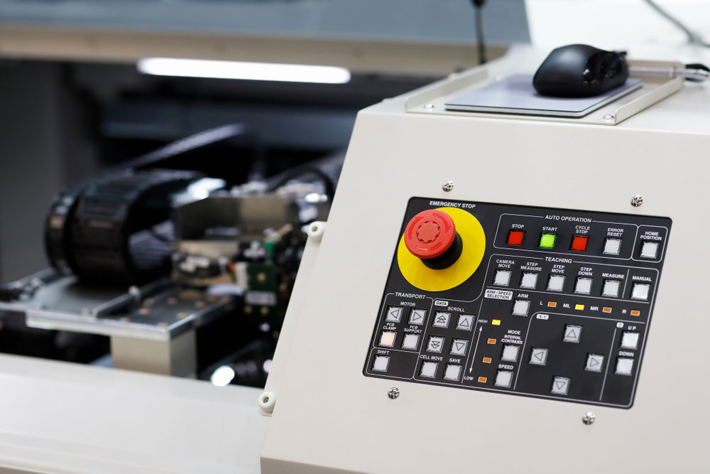
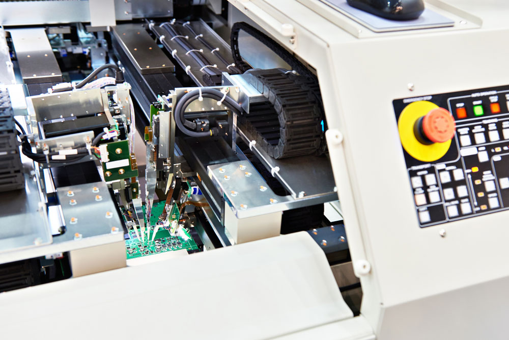
The control panel of a flying probe tester
Test Point to Board Edge Clearance
Testing machines usually have a vacuum drawdown system that secures the board to the fixture. And it requires some space around the perimeter to create a tight vacuum seal. The recommended test point-to-edge spacing is 0.125 inches to create a reliable seal. But you can reduce it to 0.1 inches minimum.
Probe Point Identification
Test machines can flag thru-hole probe points as automated test points on the board's back side. But a thru-hole pin can have a different function on the board's top side. So you should identify the probe points in silkscreen using a reference designator and a net that you can probe.
Electrical testing on a circuit board using flying probes
Probe Point Parameters
Probe points differ from automated test points, so they have unique parameters. For instance, their surface mount pad or thru-holes must be large enough to hold the loop or post that will get soldered on them. And they must be in an easily accessible location.
Wrap Up
In conclusion, PCB test points are critical for testing and detecting circuit board issues in the early stages of development. And they are essential for testing all signal lines, as shown above. We hope this article has been insightful. But if you have any questions, contact us, and we'll clarify everything asap.
Special Offer: Get $100 off your order!
Please email [email protected] for details.