FPGAs are integrated circuit hardware architectures that enable developers or users to build custom circuits to handle different computational tasks. This customization occurs via FPGA programming.
We will look at FPGA programming and how to design the primary architecture before programming. Read on to learn more!
Contents
What Is an FPGA?
An FPGA (Field-Programmable Gate Array) is a programmable chip (integrated circuit) that you can modify to perform specific tasks.
It contains input and output blocks. But its primary building blocks are configurable logic blocks (CLBs).
And these logic modules are elements like lookup tables and flip-flops.
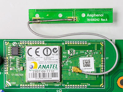
An integrated circuit mounted on a PCB
The devices used to implement these logic blocks are transistors.
So the gate arrays are silicon chips containing multiple transistors with no pre-assigned function.
These components can solve different computational problems and complex logic functions.
It is worth mentioning that FPGAs support parallelism, where the blocks can process tasks independently.
This concept makes the chips faster and more efficient, especially when data arrives quicker than the processing speed.
You can program the chip to distribute the data across multiple blocks to ensure zero lag processing.
FPGA Types
There are three FPGA types, and their functionality matches the configuration data they will process.
Antifuse FPGA
You can program these FPGAs only once to process configuration data.
They come as open circuits (fuse) and act as short circuits after programming (anti-fuse).
You cannot reverse them to open circuit status afterward for reprogramming.
SRAM FPGA
Unlike anti-fuses, you can program SRAMs several times, but this number depends on the chip model and algorithm requirements.
The FPGA stores the configuration data in SRAM, so it gets lost when you switch off the device.
A surface-mount integrated circuit
Therefore, you must reprogram the chip using data stored in external non-volatile memory every time you power it up.
The chips usually have flash memory blocks built in to provide this data.
Flash FPGA
Instead of storing the configuration data in SRAM when running, these FPGAs store it in flash memory.
So they do not need external memory elements to reprogram the ICs after switching them off. And you can program these units by changing data in the flash memory.
What Is FPGA Programming?
FPGAs are programmable devices with reconfigurable logic blocks.
So FPGA programming involves configuring or reconfiguring these blocks to solve specific computing problems.
The process requires Hardware Description Language to plan, design, and execute the gate architectures to meet the designer’s requirements.
So HDL interconnects these blocks to do specific functions, such as:
- Adders
- Dividers
- Filters
- Multipliers
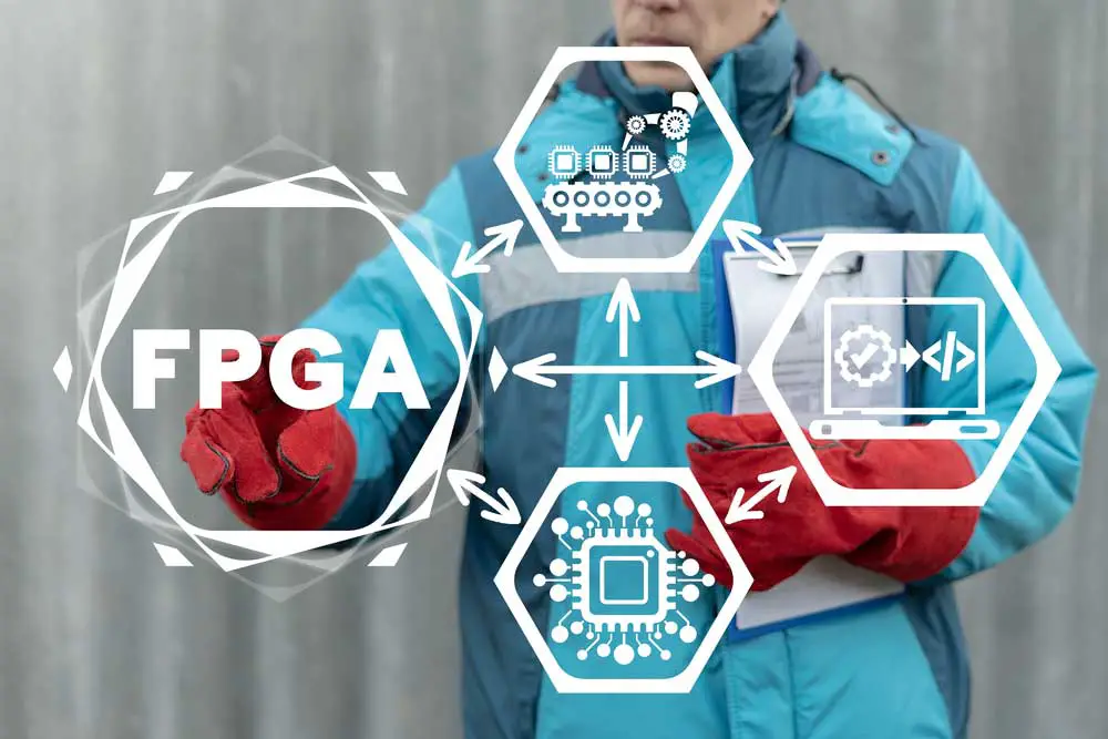
The industry concept of FPGAs
These HDLs manipulate the integrated circuits based on the device’s capabilities.
They translate the code into words and symbols that the development software converts into data to configure the chips.
Special Offer: Get $100 off your order!
Please email [email protected] for details.
Types of FPGA Programming Languages
The three typical FPGA HDLs include the following.
Verilog
Verilog is an amalgamation of two words, verification and logic. The language requires fewer lines of code to program FPGAs, so experts usually compare it to C coding language.
But some consider the language more functional for aligning the gate arrays because it is easy to learn and use.
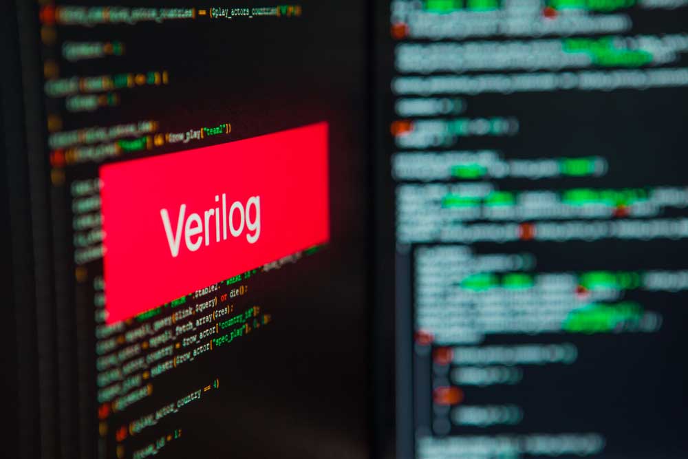
Verilog HDL programming
Verilog became the IEEE Standard 1364 and is typical in programming mixed-signal, analog, and digital circuits.
SystemVerilog
SystemVerilog began as an extension of Verilog, then transitioned to a hardware verification and hardware description language.
So you can use it to describe hardware patterns, then convert them to code to configure FPGAs.
A key difference between Verilog and SystemVerilog is their functionalities. The former can only model electronic systems.
But the latter can model, design, and test electronic systems. Currently, SystemVerilog is the IEEE Standard 1800.
VHDL
VHDL is an acronym for Very High-Speed Integrated Circuit Hardware Description Language.
The HDL started as a project for the US Department of Defense to research and build high-speed ICs. But it later became the IEEE Standard 1076.
And it is the most used language to model analog, digital, and mixed-signal circuits.
The primary advantage of VHDL is you can use it to model electronic automation.
This capability can help you determine a circuit’s output before encoding the actual hardware.
So you can check and eliminate errors before transferring the problem to the chips.
Regular Software Programming Languages vs. Hardware Description Languages
Generally, it is easy to learn new programming languages once you understand the basic concepts. But HDLs are different.
Compilers execute code sequentially when programming using languages like C and C++.
But HDLs run the code in parallel, except when handling variable assignments in VHDL processes or Verilog blocking (=) assignments.
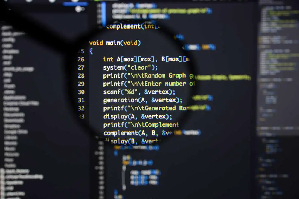
A snippet of C code written on an editor
Additionally, FPGA design involves designing digital logic circuits to model FPGA chip behavior.
But regular software programming runs a sequence of instructions to do specific behaviors.
So when starting or switching to FPGA hardware programming, forget software programming first.
Using loops and other software constructs results in poor FPGA programming behavior because these cannot model digital hardware.
Instead, you have to learn and understand logic designs and circuits.
Most things run in parallel fashion in hardware designs, which explains the parallel code execution.
So understanding parallelism is critical to developing fast and efficient digital FPGA hardware designs.
And it is vital to note that synthesis tools can take a lot of time to synthesize HDL code.
In the worst case, this synthesis process can exceed your computer’s RAM capacity.
So you might have to close the tool and execute it again.
FPGA programmers usually design the primary architectures or gates (logic circuits) before coding to avoid these synthesis delays.
So think about the function implementation and devise it before getting down to code.
How To Get Started With FPGA Programming
To get started, you must have a solid background in digital logic design.
Understand logic gates, combinational & sequential logic circuits, and logic values.
Next, select the FPGA. The applications for this IC include high-resolution video, communications, digital cameras, portable electronics, defense, space, and automotive areas.
FPGA manufacturers currently build FPGAs to match the specific user application.
So pick the most appropriate programmable chip for your project.
Also, consider the IC’s resources. These include the following.
- Complex multipliers (DSP slices)
- Internal memory capacity
- Connectivity ports
- Available IOs
- Pin compatibility
Next, estimate the resource utilization by checking the gate count and power consumption.
A chip with a lesser gate count than required is risky for the project because it won’t match the processing requirements.
FPGA architectures usually indicate the number of modules and their sub-blocks. Check these features to pick the most suitable chip.
Once you have the IC, employ this FPGA design flow to configure the building blocks.
FPGA Design Flow
This design flow has the following four stages. 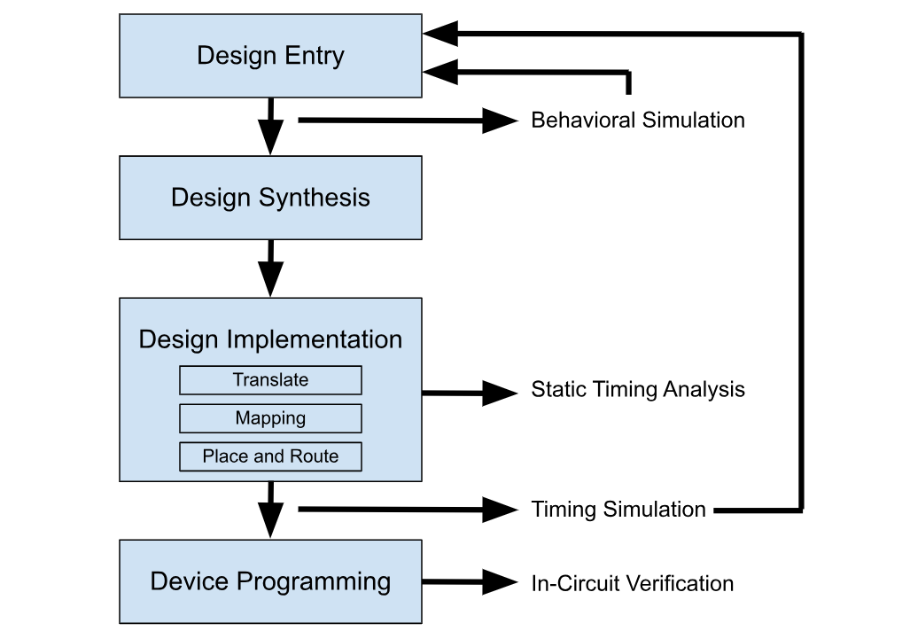
Design Entry
This stage requires entries in specific formats to go into design synthesis. The formats include:
- Schematic entries
- Simulation libraries
- RTL designs (in Verilog, SystemVerilog, or VHDL)
- Third-party IP cores
Design Synthesis
The Design synthesis involves checking the designs entered earlier to generate the logic gate netlist to implement your project.
Design Implementation
When implementing the netlist generated above, you begin with translation. This process joins all the netlists to form one native generic database (NGD).
While merging, the software checks the timing specifications and logical design rules.
And after joining, it adds constraints from the user constraint file to the netlist.
Mapping is the next step, and it involves four things.
- Processing timing and location constraints
- Generating a physical design database (or native circuit description file)
- Target optimization
- Creating a post-map STA report (shows the estimated routing and block delays)
The last substep in design implementation is placement & routing. It lists the nets and design delays in the post place & route report.
Device Programming
The programming tool creates a configuration file to match the specified settings and target FPGA. Upload this file to the chip via PROM/flash or cable to program it directly from your computer.
Vendors usually provide proprietary software to generate binary files from the nets to configure the chip. This software uploads the code via a serial interface to the FPGA. 
Advanced FPGA Design Flow
Use this advanced FPGA design flow to program chips for high-density or high-speed designs.
Here are some tools to carry out the additional steps typed in red.
- Equivalence Checks: Synopsys Formality
- FPGA Editor (altering the routing and placement): Xilinx FPGA Editor
- Power Calculation: Xilinx Xpower
- Static Timing Analysis: Synopsys Primetime
FPGA Programming Tips
- Use an FPGA development board to familiarize yourself with FPGA programming. It is like using an Arduino board to understand microcontroller programming. Using FPGA dev boards is difficult at first, but practice makes perfect.
- Begin with something simple like you would start with “Hello World” in software programming languages.
- Familiarize your design and programming with the target FPGA chip. Check the configurable logic blocks and figure out how to incorporate them into your design.
- If working in sequential circuits, learn how the clocking nets work.
- Verify the FPGA designs in simulations before uploading the code into the chip to minimize the long synthesis periods.
Wrap Up
Programming FPGAs is not a straightforward process. Even experienced software developers will find it challenging because the coding process differs from software programming.
But you can learn using FPGA dev boards and design the hardware architecture before coding to simplify the process.
Special Offer: Get $100 off your order!
Please email [email protected] for details.