PCB manufacturing primarily involves etching a copper sheet plated to a non-conductive substrate and drilling through holes. These holes connect the different copper layers in the board or components attached externally. However, the holes will not be conductive until a thin layer of copper gets electroplated to the hole walls. Once this happens, you get a PTH PCB. We will look at this technology and how it stacks up against its non-plated counterpart below.
Contents
- How to Define PTH and NPTH in PCB Design?
- What is PTH?
- What is NPTH?
- PTH vs. NPTH: The Difference Between Making NPTH or PTH for the PCB Factory
- PTH Components Handling Processes
- Drilling Rules for NPTH and PTH PCBs
- NPTH PCB(Non-Plated-Through-Hole PCB) Drilling Hole Rules
- PTH PCB (Plated-Through-Hole PCB) Drilling Hole Rules
- Reasons for PTH PCB Failure and Their Solutions
- Solutions
- Surface Mount (SMT) vs. Plated Through-Hole (PTH)
- Surface Mount (SMT)
- Plated Through Hole (PTH)
- Advantages of PTH Production
- Typical Applications For NPTH/PTH
- Milling slots for Voltage Isolation Air Gaps
- Plated Slots for Parts with Square/Rectangular Component Connections
- How to Lower Through Hole PCB Cost?
- Using Larger Annular Rings
- Reducing the Hole Density Per Square Meter
- Drilling Larger Holes
- Summary
Special Offer: Get $100 off your order!
Please email [email protected] for details.
How to Define PTH and NPTH in PCB Design?
PTH and NPTH are synonyms for Plated Through Holes and Non-Plated Through Holes, respectively. The two refer to the following.
What is PTH?
For a hole to qualify as a PTH, its copper pad and solder stop mask should be larger than the hole diameter (overlay it with 6-mil minimum width).
What is NPTH?
NPTH slots do not meet the prerequisites of PTH. A hole qualifies to be NPTH if it meets the following conditions.
- The copper pad's size is tinier than the hole, and sometimes, there's no copper.
- The pad's copper overlay exceeds the hole size but with a 6-mil buffer zone between the slot and copper.
PTH vs. NPTH: The Difference Between Making NPTH or PTH for the PCB Factory
Another way to differentiate between the two is that PTH drilling occurs before the electroless copper process while NPTH drilling occurs after that. While defining the two is straightforward, designing them in a circuit board layout can be tricky.
For instance, a file showing the pad's copper overlays and is wider than the hole but with no solder stop mask is confusing. Should the manufacturer plate it or not?
Therefore, you should pay close attention to the Gerber files before sending them for PCB fabrication.
Here's an example. From the manufacturer's point of view, if all drills have a solder stop mask that overlays and is larger than the hole:
- Those qualifying to be PTH have connections to the copper traces, and their copper pads are broader than the hole
- Those with no copper are Non-Plated (NPTH)
PTH Components Handling Processes
The leads of electronic components get inserted into the PTH PCB using one of the following automated processes.
- Axial insertion for diodes and resistors
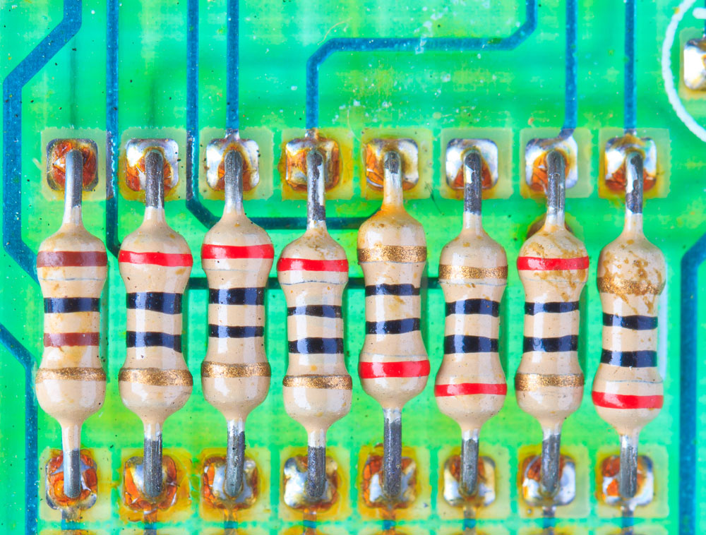
Resistors soldered to a PCB
- Radial insertion for electrolytic capacitors
- Odd form insertion for transformers, connectors, etc.
- Manually for other components
After insertion, the thru-hole components get soldered using one of these soldering techniques.
- Hand soldering
- Wave soldering (intrusive reflow process)
- Selective soldering.
Soldering during PTH assembly forms sturdier joints than the ones created in SMT assembly because the leads go through the PCB.
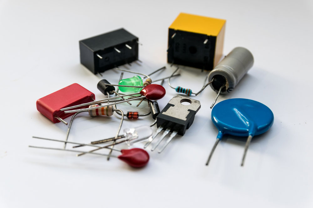
PTH components
Drilling Rules for NPTH and PTH PCBs
When designing and manufacturing NPTHs and PTHs, consider the following rules.
NPTH PCB(Non-Plated-Through-Hole PCB) Drilling Hole Rules
- 6-mil minimum complete hole size
- 5-mil minimum edge-to-edge clearance from all other surface elements
PTH PCB (Plated-Through-Hole PCB) Drilling Hole Rules
- 4-mil minimum annular ring size
- 6-mil minimum complete hole size
- 9-mil minimum edge-to-edge clearance from all other surface elements
Generally, consider the via types, drill hole sizes, aspect ratio, and spacing when developing the drill hole DFM rules and guidelines. For instance, if your Design For Manufacturing (DFM) purpose is saving space, use via-in-pads.
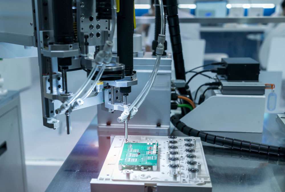
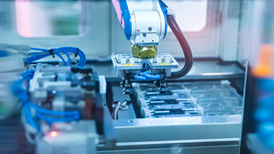
Robot PCB Drilling
Special Offer: Get $100 off your order!
Please email [email protected] for details.
Reasons for PTH PCB Failure and Their Solutions
A PTH assembly can experience the following failures.
- ICD (Interconnection Defect)
- Barrel cracking
- Foil cracks
- Barrel cracks
- Thermal excursion stress
However, the biggest issue experienced during the PCB manufacturing process is ICD. It occurs due to the stress caused by differences in CTE (Coefficient of Thermal Expansion) and the PTH system.
Glass reinforcement on the resin limits expansion on the X and Y axis. Therefore, the material expands faster along the Z-plane. This movement stresses the adhesion between the plated copper and its interconnections and can cause separation.
The same stress causes other issues, which can occur simultaneously or gradually over multiple cycles.
Solutions
First, ensure you adhere to the best copper plating practices. Second, try the following solutions.
- Maintain the electroless copper thickness on all plated copper interconnections
- Ensure the copper structure grain deposit is sturdy
- Choose a resin material with a high Td (high temperature for decomposition) to handle thermal strain without losing resin material weight
- Test the high aspect-ratio through-hole circuit boards by subjecting them to repeated thermal shocks during prototyping. The goal is to identify the temperature range at which failure occurs.
Surface Mount (SMT) vs. Plated Through-Hole (PTH)
PCB electronics are mostly either SMT or PTH, and these compare as shown below.
Surface Mount (SMT)
SMT components are the most typical types in modern electronics because they are cheaper, tinier, and easier to assemble. SMT assembly involves high-speed placement using a pick-and-place machine followed by soldering using a reflow oven.
While this automation makes it easy to mass produce SMT, the tiny component size complicates hand/manual assembly. Also, you will need more equipment (hot air rework station or reflow oven).
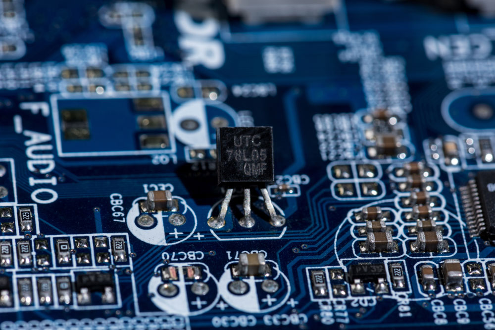
Several SMT components and one through-hole component are soldered on a PCB. Note the size difference.
Why Use SMT?
- If you need a small design
- For mass production
- If the chips/components you need are not available in PTH packages
Plated Through Hole (PTH)
PTH components are the most typical type used for hand soldering. Usually, they feature wires or leads (two or more) that fit into the component holes in the PCB. You can also stick these pins into breadboards when prototyping.
These electronic components are usually larger than their SMT counterparts, so they are seldom used in the ever-shrinking consumer electronic PCBs.
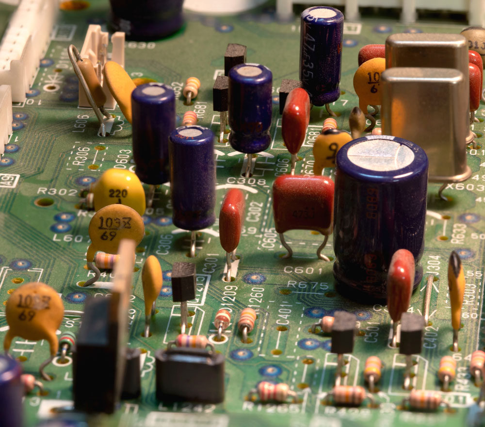
Through-hole components soldered to a PCB
Why Use PTH?
- For prototyping (using a breadboard)
- If the project is for a small production run
- For sturdy attachment of bulky and heavy components like transformers
Advantages of PTH Production
- Sturdier mechanical bonds in the PTH PCB assembly than with SMT assembly
- Possible to repair faulty connections individually by hand instead of replacing the entire circuit
- PTH assembly is ideal for bulky components
Typical Applications For NPTH/PTH
PTHs and NPTHs have several applications, but the following are the two typical ones.
Milling slots for Voltage Isolation Air Gaps
Electrical arcs can occur temporarily between some high-voltage copper traces. These arcs can cause carbonation when they frequently occur, leading to short-circuiting. However, arcing over a milling slot doesn't cause carbonation.
Plated Slots for Parts with Square/Rectangular Component Connections
Components like DC jacks with non-rounded leads require plated holes. The reason is that the space between the peg and hole wall will be solder-filled, creating a reliable joint.
How to Lower Through Hole PCB Cost?
One of the disadvantages of Through Hole plating is its high cost. But you can reduce the manufacturing costs by:
Using Larger Annular Rings
The minimum annular ring size is the border of the hole's and pad's minimum distance. It is a critical requirement that refers to the vias and through-hole pads. PCB manufacturing costs increase if the minimum annular rings are smaller than the standard requirements.
Reducing the Hole Density Per Square Meter
Laser or mechanical drilling machines have a specific operating efficiency. Therefore, drilling a higher hole density on a PCB will require more time. If your project allows you to decrease the hole density, you can hasten the board manufacturing process and lower costs during mass production.
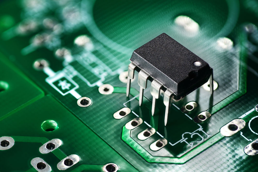
PTH Printed circuit board and chip
Drilling Larger Holes
Tiny hole drilling requires expensive high-precision machines. Manufacturers usually recover these costs from the buyers by charging more for drilling holes with diameters between 0.15mm and 0.3mm. Therefore, drilling larger slots can significantly reduce the costs.
Summary
There you have it! Although PTHs are rare or not present in modern consumer electronics, they have some unique applications that keep them relevant in PCB design and production. We hope this article has been insightful. If you think we left something out or have any questions/comments, leave a message, and we'll respond shortly.
Special Offer: Get $100 off your order!
Please email [email protected] for details.