High-speed printed circuit boards require reliable transmission lines for sending signals from transmitters to receivers. These lines come in different types and have varying properties & parameters that affect signal transmission. Here is an in-depth look at the PCB transmission line, including signal behavior prediction on the electrical paths. Take a look!
Contents
- What is a PCB Transmission Line?
- Types of Transmission Lines
- Microstrip
- Stripline
- Coplanar
- Properties of a Transmission Line
- When is an Interconnection Considered a Transmission Line?
- Impedance Control on Transmission Lines
- Predicting Signal Behavior on Striplines and Microstrips
- Signal Speed
- Materials Used in PCB Transmission Lines
- What is the Critical Length of the Transmission Line
- What is the Allowed Mismatch Level?
- Wrap Up
What is a PCB Transmission Line?
A PCB transmission line is an interconnection between transmitters and receivers for moving signals from the former to the latter. It consists of two PCB traces, the first being a signal conductor and the second a return path conductor (usually a ground plane). Between the two traces is the dielectric material.
Transmission lines on a microwave PCB
Types of Transmission Lines
The following are the three types of transmission lines in PCBs.
Microstrip
A microstrip transmission line consists of a single signal uniform trace routed on the outer layer of the PCB. This signal trace runs parallel to the conducting ground trace, with the dielectric material separating the two via a certain height or thickness.
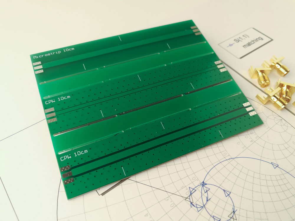
An RF signal transmission line on a PCB. Note the 10cm microstrip.
Stripline
A stripline features an internal signal trace surrounded by a parallel PCB dielectric layer on both sides. Two outer ground planes run parallel to the signal trace, so this transmission line has two return paths.
Coplanar
Coplanar transmission lines contain an external signal trace flanked by ground/reference planes on both sides. Therefore, the coplanar waveguide structure has three conductors on the same PCB layer with the PCB dielectric board material underneath.
Strip lines and microstrips can have a coplanar structure. The typically used coplanar waveguide configurations include:
- Coplanar waveguide with the ground
- Coplanar waveguide
Coaxial cables are not types of PCB transmission lines, but they qualify as transmission lines outside PCBs. Therefore, coaxial transmission is ideal for high-frequency applications, such as music and TV.
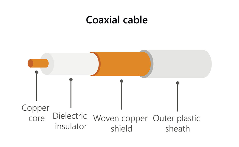
A coaxial cable
Properties of a Transmission Line
A transmission line has two vital properties: propagation delay/ unit length and characteristic impedance. Crosstalk, signal reflections, and electromagnetic noise will occur if you don't do the following.
- Control the impedance along the length of the transmission line
- Terminate the line by the correct impedance value
Therefore, it is crucial not to ignore transmission line effects to avoid these factors because they degrade the signal quality and interfere with the signal integrity.
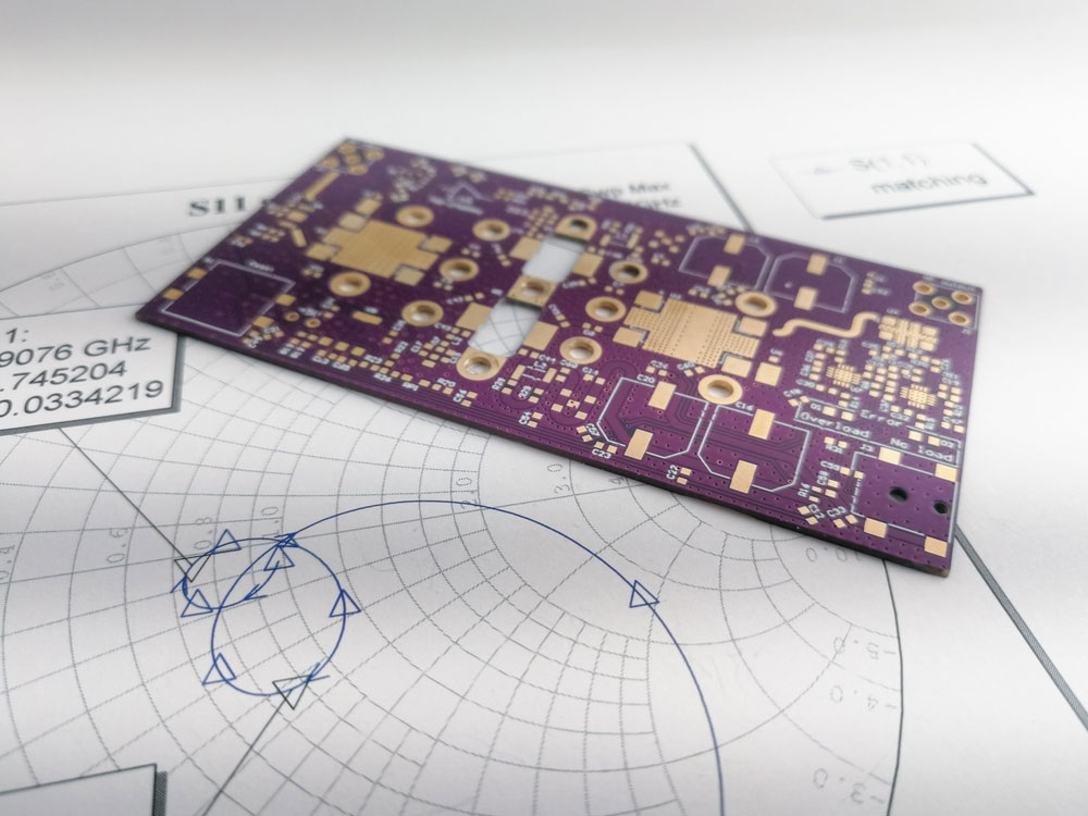
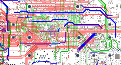
A high-power RF PCB on a Smith chart for impedance matching
Also, it is critical to consider the transmission line parameters like inductance, resistance, conductance, and capacitance when analyzing transmission lines.
Special Offer: Get $100 off your order!
Please email [email protected] for details.
When is an Interconnection Considered a Transmission Line?
When signal frequencies for analog signals or data transfer rates for digital signals are below 50MHz or 20Mbps, the signal propagation time from source to destination will be short. It will be less than 10% compared to one-fourth of the wavelength of the analog signal or the fastest rise time of the digital electrical signal. You can analyze these low signal speed scenarios using conventional network analysis techniques while ignoring the transmission line reflections or signal propagation time.
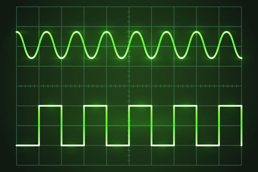
Analog vs. digital signal wave diagrams on an oscilloscope
But when dealing with high-speed signals (high frequencies and data transfer rates), you cannot ignore the signal propagation time compared to one-fourth of the wavelength or quickest pulse rise time. Therefore, you cannot analyze this high-speed signal behavior using typical network analysis techniques. These interconnections are high-speed transmission lines and require analysis as transmission lines.
Impedance Control on Transmission Lines
The alternating current signal running on PCB transmission lines has a frequency high enough to show its wave propagation nature. A transmission line has an impedance at each point, and the line impedance is uniform if the line geometry is the same along its length. Such a line is a controlled impedance line.
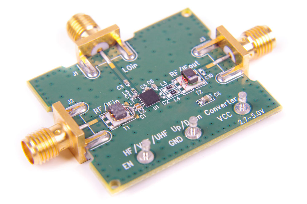
A radio frequency microwave mixer evaluation board
Non-uniform impedance causes signal distortion and reflections. So at high frequencies, transmission lines should have a controlled impedance to predict the signal behavior.
Predicting Signal Behavior on Striplines and Microstrips
Here are a few calculations to determine the signal speed and propagation delay for striplines and microstrips.
Signal Speed
The speed of signals is slower when moving through a circuit board's transmission line than when propagating through a vacuum or air.
Why?
The dielectric constant of the fabricated board's dielectric material affects them.
Therefore, the formula for calculating the signal speed is as follows.

Materials Used in PCB Transmission Lines
The following is a breakdown of the signal speeds and propagation delays through the typical dielectric materials compared to the transmission through air/vacuum.
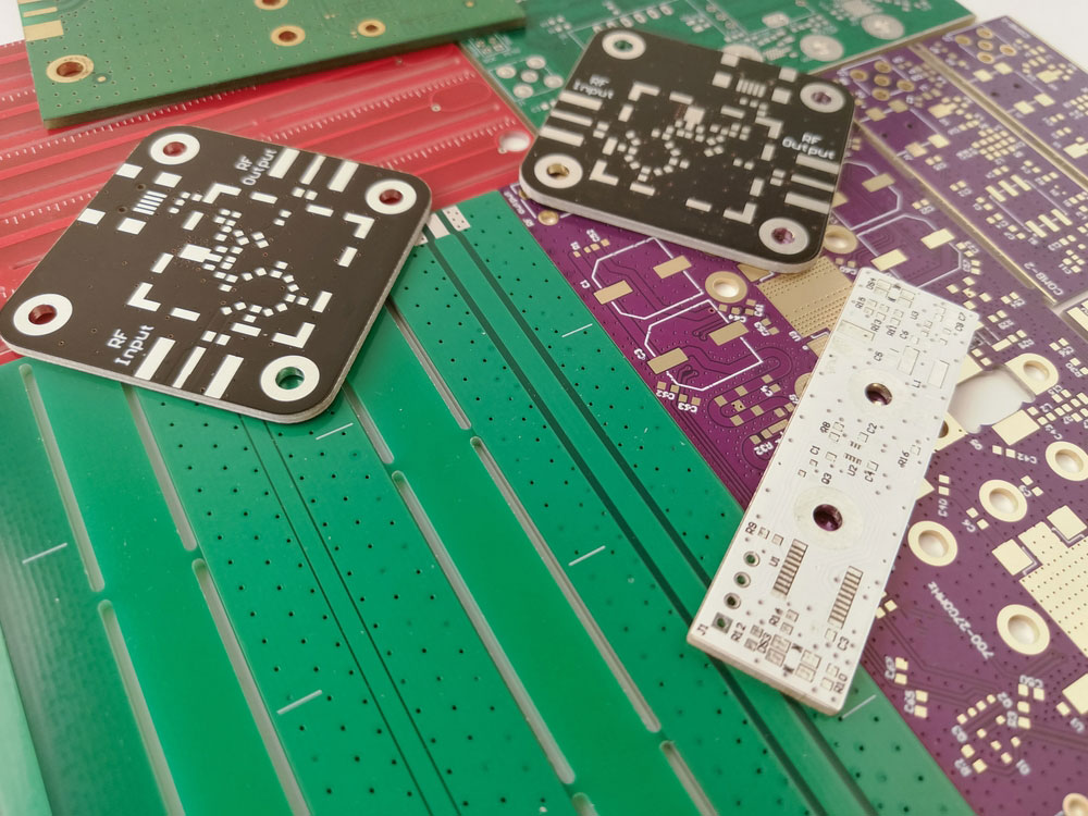
Various printed circuit boards were built for radio frequency projects.

What is the Critical Length of the Transmission Line
The critical length is one-fourth of the highest signal frequency's wavelength in a signal (for analog signals). But the quickest rise/fall time (transition from one logic level to another) is more important for digital signals. Therefore, the critical length is the line length across which the signal propagation time is half the quickest rise/fall duration of the pulses.
Signals behave as if they move with an impedance closer to the load impedance if the transmission line is short. As the line becomes longer, it acts as if its impedance is closer to its characteristic impedance.
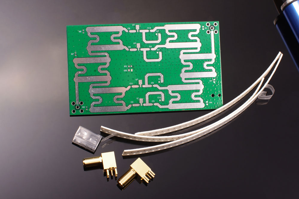
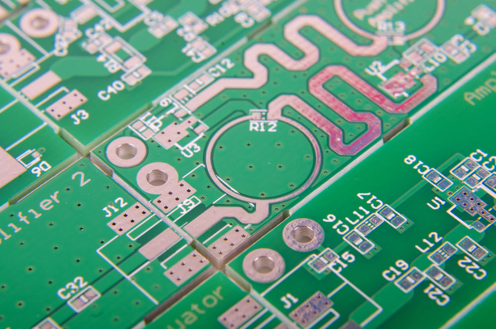
A radio frequency and microwave PCB assembly
The transition region from the load to characteristic impedance depends on the following.
- Losses in the system (lossy transmission)
- Acceptable impedance mismatch between the source, transmission line characteristic impedance, and load
It is best to match these impedance parameters to the same value. The input/source impedance is the impedance signals come across after transients decay to zero. It is a characteristic impedance when you match the load and line impedance regardless of the line length.Also, you don't have to worry about a voltage stair-step increase in digital signal loads if the reflection coefficient is zero. In the case of analog signals, you won't have to worry about standing waves developing on the line.
What is the Allowed Mismatch Level?
As you can see, the impedance mismatch weighs heavily on the line's critical length. And the allowed mismatch level depends on the permissible variation level tolerated in the input impedance away from the load impedance.
For instance, a 10% change in the input impedance can occur if the line length is a tenth of the signal wavelength. Therefore, if the input impedance's tolerable deviation is 10%, the critical length will be a tenth of the wavelength.
The critical length is also sensitive to system losses (conductor and dielectric losses), so you can multiply the losses by 10.
Wrap Up
In conclusion, PCB transmission lines are critical when creating high-speed designs for PCBs. The most typically used types are microstrips and striplines, and you can use the signal prediction behavior described above to determine the best PCB layout for your project. We hope this article has been insightful. If you have any questions or comments, reach out for further clarification.
Special Offer: Get $100 off your order!
Please email [email protected] for details.