Many power supply types with different capabilities exist on the market today. These may feature complex circuit designs suitable for their intended purpose. Some can even convert one power type into another, such as AC to DC. Of course, those also offer different performance processes, mainly when supplying power. You can even utilize them for all sorts of applications requiring high voltage. So let’s take a look! This article will introduce the flyback converter, a power supply that converts AC into DC with unique components.
Contents
- What Is A Flyback Converter?
- Flyback Converter Basic Components
- Overall, A flyback Converter Relies on These Three Components to Operate Efficiently:
- Flyback Converter Operation
- Flyback Converter Design and Component Selection
- Step one: Design
- Step two: Maximum primary inductance calculations
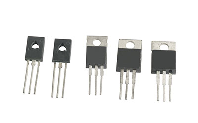
- Step three: Calculating MOSFETs
- Step four: Calculating the rectifier diodes
- Step five: Calculating output capacitor
- Step 6: Flyback transformer
- Step 7: Snubber design
- The circuit
- Advantages of the Flyback Converter
- Applications of flyback converters
- Summary
What Is A Flyback Converter?
A flyback converter refers to a power supply topology with AC to DC conversion capabilities. Generally, this power converter stores energy via the coupled inductor as current flows through its circuit. It also releases that energy after cutting off power. Also, it operates as a switching mechanism for step-up or step-down voltage transformers. Rather than an inductor, the transformer features a primary winding. Meanwhile, the secondary serves as the output. In this case, both the primary and secondary windings remain isolated.
Flyback Converter Basic Components
Overall, A flyback Converter Relies on These Three Components to Operate Efficiently:
- Flyback Transformer:
A flyback transformer works by storing energy in the primary magnetic field. After a specified period, the component will distribute that energy to the secondary.
- Switch:
The switch’s purpose involves powering the primary circuit on and off, causing the transformer to magnetize and demagnetize. Overall, a selected controller’s PWM signal controls the switch.
- Rectifier and Filter:
Lastly, the rectifier converts the secondary winding’s voltage into direct current voltage. Afterward, the capacitor blocks the voltage to boost the DC value. It will also prevent the load from reaching the secondary winding.
Special Offer: Get $100 off your order!
Please email [email protected] for details.
Flyback Converter Operation
A flyback converter features similar mechanisms as many switching converter topologies. These contain a coupled inductor, which isolates the input from the output. Also, the converter’s tON and tOFF semi-period signals control the switching state.
While in tON, the MOSFET activates, allowing the coupled inductor to charge via current flow sourced from the input. On the other hand, tOFF deactivates the MOSFET, causing the diode to demagnetize the coupled inductor. The load receives power through the capacitor, which charges via the inductor’s current.
Flyback Converter Design and Component Selection
Designing a flyback converter usually requires you to consider various designs and accommodations. The steps below will guide you through the entire process.
Step one: Design
Design inputs include power, operation mode, input voltage, and ripple factor. The table, as shown below, demonstrates the value for each parameter in the circuit.
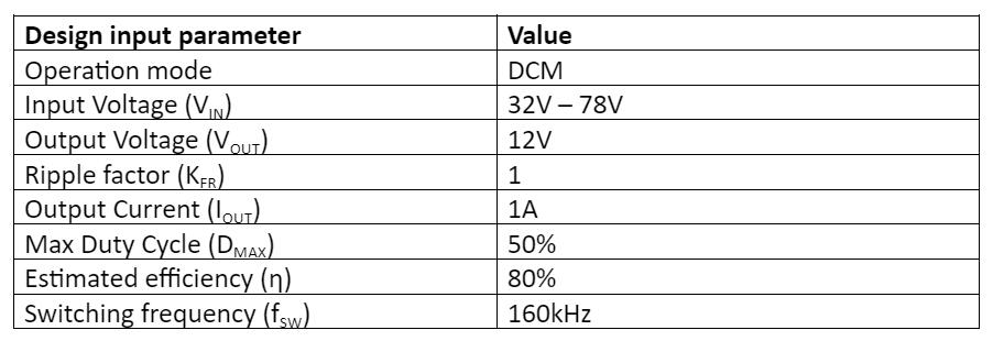
This circuit relies on the DCM (discontinuous conduction mode) for improved stability and efficiency. As a result, the ripple factor sets to one. Also, the max duty cycle sets to 50% to reduce stress while allowing both the diode and MOSFET to operate. Meanwhile, the switching frequency has a 160kHz value.
Configuring the estimated efficiency to 80% ensures the converter can perform realistic calculations. It comes with primary-side regulation. A designer will need to select a controller IC to meet the above parameters. For this reason, you should utilize the MPS MP6004 flyback controller.
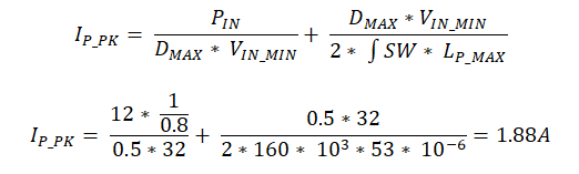
Step two: Maximum primary inductance calculations
First, you will need to calculate the maximum primary inductor. Use the equation below, which accommodates the DCM mode, for this purpose:

If the converter entirely operates with a max duty cycle and minimum input voltage, it will cause a worst-case scenario. Integrating the design inputs from the above equation sets the max inductance to 53 μH.
You will need to apply the minimum VIN and max D. Adding the diode’s forward voltage drop provides a more accurate calculation. Afterward, you will need to calculate the turn ratio (nS1). Use the following equation to calculate nS1:

Step three: Calculating MOSFETs
Next, you will need to utilize the correct MOSFET for this project. It involves calculating the max voltage and current for the switch. You can do this with the following formula:

The 20% safety margin helps maintain safe operation for the component. Use the equation below to calculate the max current:
Also, you can utilize the MP6004 controller for this project. Its VDS_MAX value sets to 180V while the max current sets to 3A.
Step four: Calculating the rectifier diodes
This step involves calculating the maximum voltage the rectifier diodes can handle. Use the following equation to determine that value:
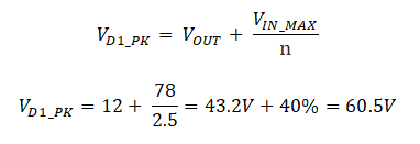
The maximum reverse voltage equals 60.5V with an added 40% safety margin.
Step five: Calculating output capacitor
Ignore the output crosstalk and parasitic components for this step. Use the following equation to calculate the capacitor’s voltage:
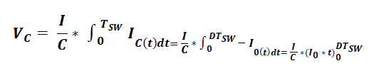
Meanwhile, the following formula determines the output voltage ripple.

Lastly, utilize a 250µF capacitor, which configures 12.5mV, for the output ripple voltage.
Step 6: Flyback transformer
When choosing the transformer, you must consider the core shape and material. So select the double E ferrite core transformer for this project. The AP method generally refers to the transformer’s total area. It refers to the winding window area (AW) and the core-cross section area (AE). You can calculate the transformer’s size with the following equation:

Afterward, refer to the following equation to determine the minimum transformer area:
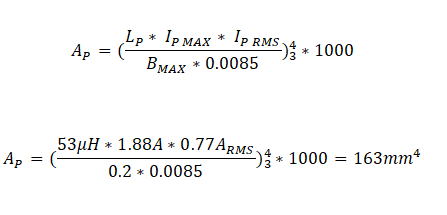
The transformer’s ferrite core BMAX input parameter values are between 0.2T and 0.3T. Utilize an EE13 core and a 0.28mm long bobbin for this purpose. Next, calculate the primary turn number with the following equation:

Use the following equation to calculate the secondary turn number:

Lastly, refer to the second turn number methodology to determine the auxiliary winding turn number. In this case, NAIX will equate to five.
Step 7: Snubber design
The final part of this project involves determining each snubber value. Adding a snubber ensures that the voltage spikes weaken. Otherwise, these spikes will generate noise, potentially damaging the MOSFET.
Overall, the snubber features three stages. The first involves setting the leakage inductance to two percent of the primary. Afterward, the maximum snubber capacitor voltage ripple configures to ten percent. Lastly, you can calculate the snubber components’ values.
Use the equation below to determine the maximum capacitor voltage:

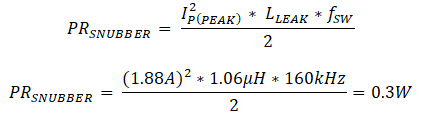
Then, calculate the snubber resistor’s power with the equation:
Next, determine the snubber resistor with the below formula.

Use the following equation to determine the snubbing capacitor:

Finally, determine the snubber diode’s max voltage:

The circuit
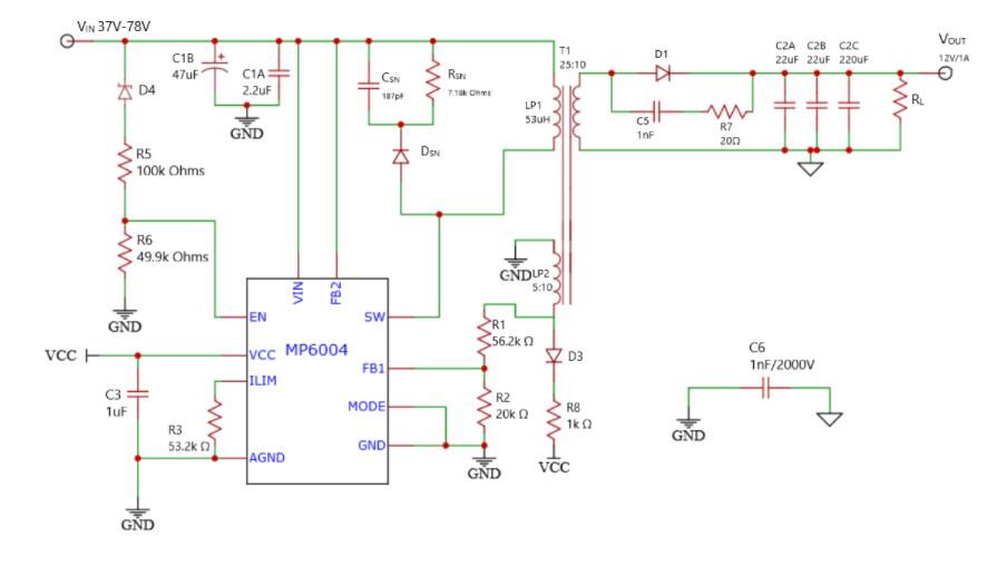 Flyback converter circuit diagram.
As a whole, the circuit includes the auxiliary inductor (LP2), primary inductor (LP), rectifier diode(D1), output capacitor )C2A, C2B, C2C), and snubber circuit. You can integrate the MP6004 with the other components after performing each calculation. This will lead to a fully operational flyback converter.
Advantages of the Flyback Converter
The benefits of flyback converters include:
- Primary stays isolated from the output.
- Relies on minimal components versus other SMPSs
- Works with many different voltage levels
- Can supply several output voltages
- An individual control mechanism can regulate multiple output voltages.
Applications of flyback converters

CRT monitors generally feature a flyback converter.
You Can Utilize a Flyback Converter for Many Different Applications. We Listed a Few Below:
- Standby power supplies for computers
- Cell phone and mobile device chargers
- Low-power consumption TVs and PCs (250W)
- Isolated gate drive circuits
- High voltage supplies for lasers, CRTs, televisions, Xenon flashlights, copiers, and more
- Input-output power supplies
Summary
The flyback converter is an excellent power supply that converts AC into DC PO er. It generally works differently compared to other devices. At the same time, it also features specific components to help it perform properly. For example, the transformer ensures that it can store energy in the magnetic field. Thus, it makes it efficient for power distribution and conversion purposes.
Do you have any questions regarding power convert rs? Feel free to contact us!
Special Offer: Get $100 off your order!
Please email [email protected] for details.