Soldering is a critical process during component assembly on a PCB. But several factors can cause poor solder joints when soldering manually or automatically. One of them is excessive heat transfer from the solder pad or thru-hole. This issue makes it difficult to attain the required temperatures to melt the metal. You can solve this issue using a thermal pad, which minimizes heat dissipation. We will look at a thermal pad PCB in detail and show how it assists in the soldering process. Let's get right into it!
Contents
Special Offer: Get $100 off your order!
Please email [email protected] for details.
What is a Thermal Pad?
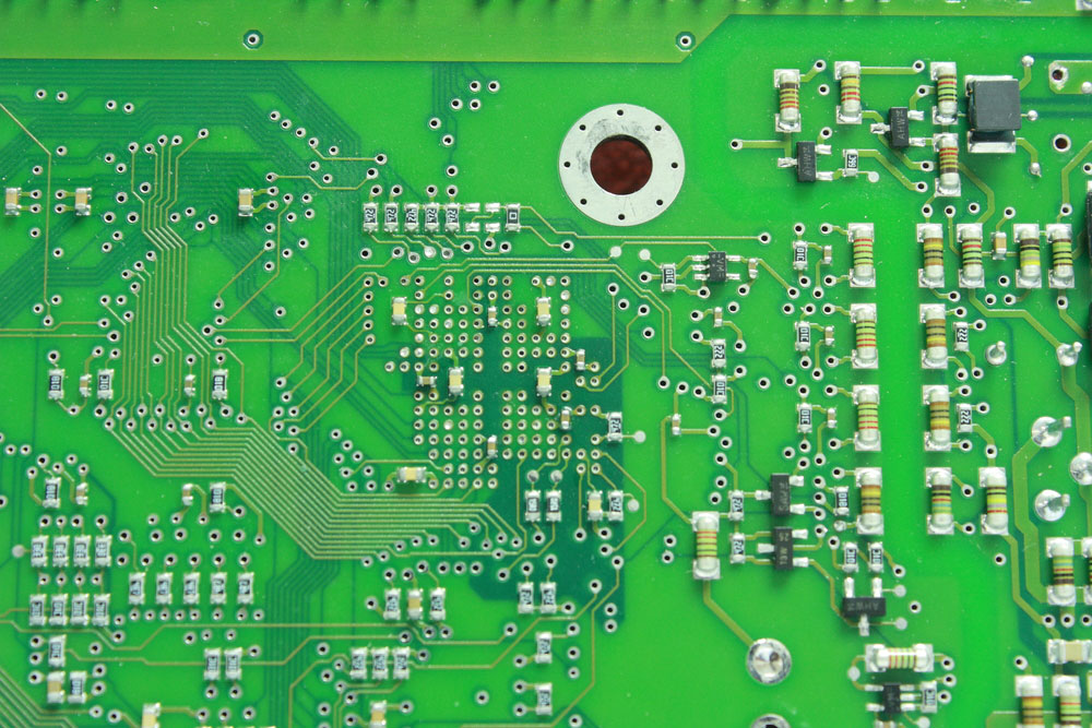
A thermal pad is a PCB pad connected to a copper surface (copper pour) via a thermal connection through four traces or spokes. The thermal relief pad resembles a regular PCB pad but has copper spokes linking it to the surrounding copper plate.
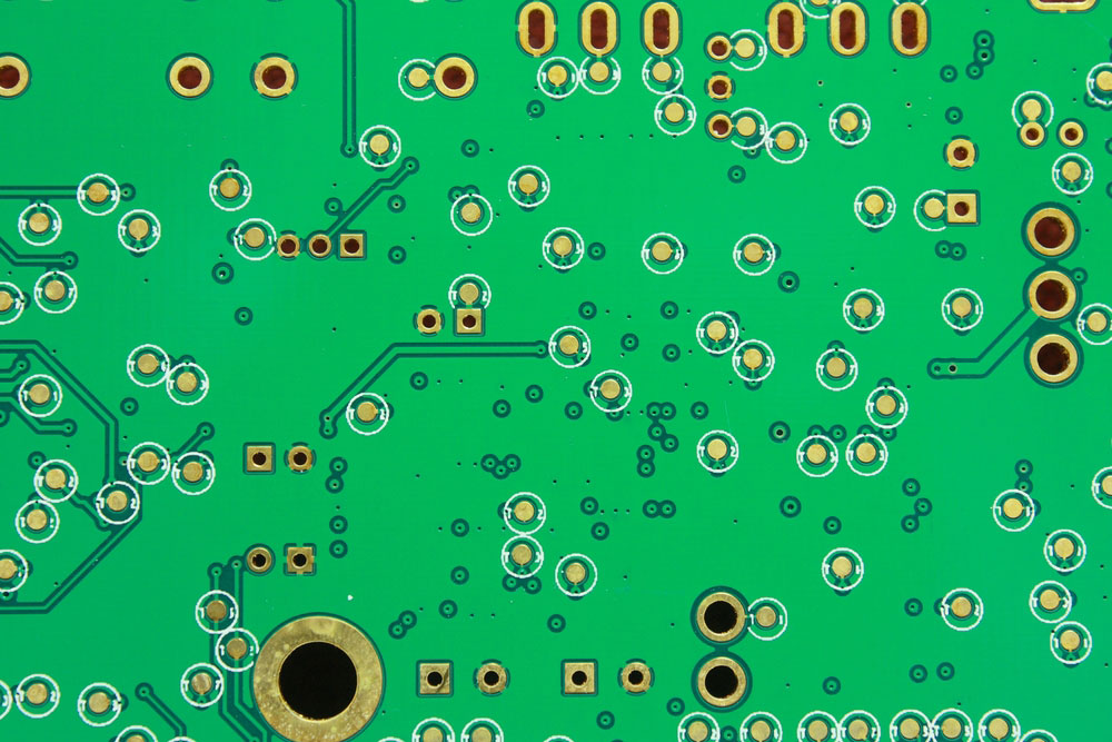
A PCB board with several pads. Note the thermal pad with spokes on the upper left section.
Thermal Relief Pad Functions
Thermal reliefs aid in the assembly process of circuit boards. A regular pad has a large, exposed copper area that increases the surface area for heat to escape to the metal plane. The metal section acts as a heat sink, so it causes the solder alloy to melt slowly. Also, it can cause poor solder joints because it draws heat away from the pin during automated soldering.
However, having too much metal on one pad (a regular pad) vs. the spoked metal pad can be an issue when soldering SMT components across them. Since one PCB pad loses heat faster than the other, it can cause a thermal imbalance. This imbalance causes tombstoning. Tombstoning is a manufacturing phenomenon where one side of the soldered component lifts partially from the pad.
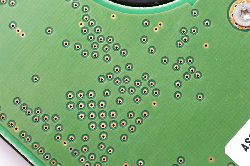
A PCB with several thermal pads
But since thermal relief pads contain spokes or metal traces, these power lines must be thick enough to handle the current passing through them. Therefore, it is crucial to balance the number and widths of the spokes to create a good thermal pad design.
Tiny spokes might not conduct enough current. But if they are too broad, they might pull a lot of heat away from the pad.
Special Offer: Get $100 off your order!
Please email [email protected] for details.
PCB Thermal Pad Layout Guidelines
Thermal pads are necessary for certain aspects of the PCB layout, and you should consider them in the following four areas.
Surface-Mount Pins
Most designers embed surface-mount pads in metal fills because this connection enhances electrical performance. But this metal fill pulls heat away from the metal pad. And if the pads belong to a tiny 2-pin discrete part, the solder on the other pad will melt faster than the one on the embedded pad. The surface tension caused by the uneven melting will cause the tombstoning phenomenon explained earlier.
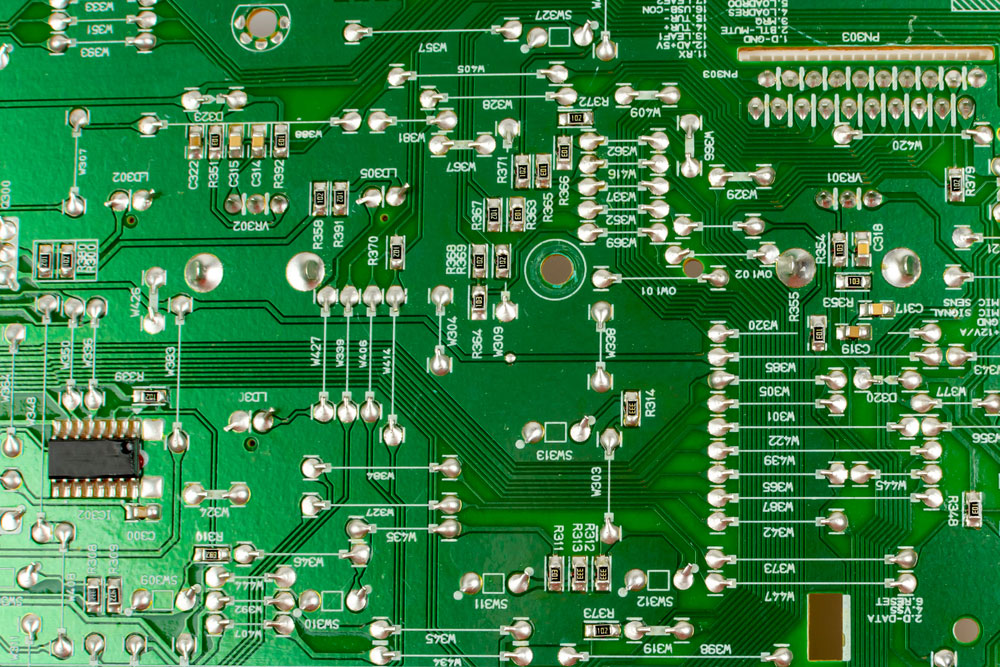
A circuit board with several components attached
Instead of embedding the surface-mount pad, you can use multiple traces to connect to it. These traces will balance the heat on both metal pads when soldering.
Thru-Hole Pins
Holes for thru-hole components are the ideal candidates for thermal relief pads. Large multi-layer boards with several ground planes can have thru-hole component pins connecting to several square feet of metal. This connection requires a solid solder joint to create reliable electrical links.
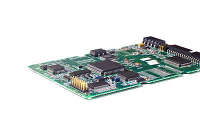
A computer’s mainboard with several components attached
Tiny metal areas, such as split planes, can act as heat sinks, drawing heat away from the thru-hole component pin. Therefore, you will require excessive heat to create a solid solder joint. This excess heat can cause damage to nearby traces and components.
Thermal relief pads will reduce heat-sinking effects, enabling you to solder thru-hole components without causing damage.
Vias
Most vias connecting to ground and power planes don't require thermal relief pads because no pin gets soldered inside. But with power nets that transmit high currents, short traces can still conduct a lot of heat to the surface-mount pins. In this case, thermal reliefs are necessary.
Vias in a PCB
Metal Routing
Thermal pads are necessary for connecting component pins to large fill areas or power and ground planes. But you must consider their application on power trace routing for each case.
Power traces conducting low-current loads can have narrow transmission lines. CAD systems that add thermal reliefs automatically to pins on nets can ruin the design. The copper spokes might have little room to connect, resulting in a connection lacking enough metal.

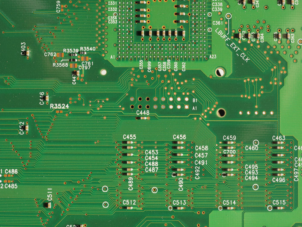
PCB trace routing in the layout stage
It is vital to note that the number of thermal relief pads (and their widths) should match the trace width as dictated by its power requirements. For instance, if routing a 50-mil power trace but can only get two spokes, each five mils wide, you won't have enough metal for the connection.
The power flowing through the restricted pathway can produce significant amounts of heat during operation due to resistance. Eventually, the extra heat will burn out the connection.
On the other hand, more metal in the traces will create a lower net inductance that keeps the EMI under control. Therefore, you should create thermal pads with just the required amount of metal in the trace connections. Using the earlier example, you should have four 12.5-mil traces to match a 50-mil power trace.
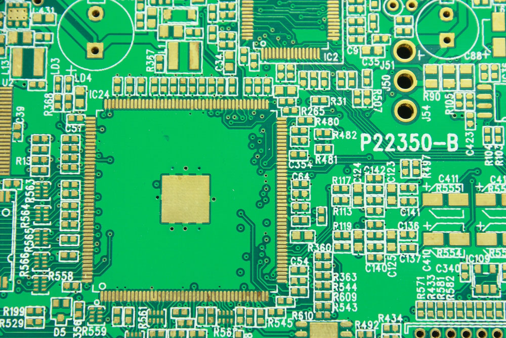
A microcircuit close-up of a PCB
CAD Systems Design Rules
CAD systems have built-in design rules for thermal relief pads that you need to understand and set up. These rules determine the size, number, shape, width, and minimum number of allowable spokes. Also, you can apply these connection rules to the individual nets, component classes, pins, or net classes.
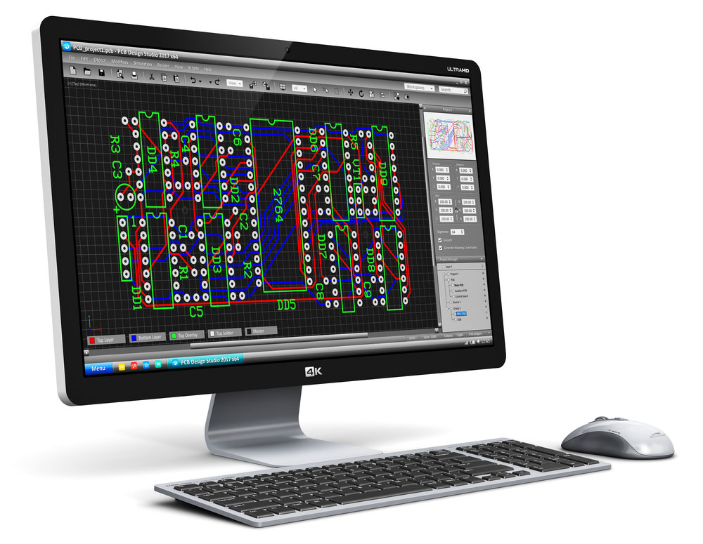
A PCB design in CAD software on a computer
In some cases, the thermal relief pad might not be able to connect its spokes/traces correctly. It typically happens when the PCB pads have the following characteristics.
- Get congested together
- Are in a split plane
- Are in a small metal area
Therefore, you should ensure the PCB design software has rules to detect the minimum thermal relief connections. Also, keep an eye out for these issues.
How Your PCB Manufacturer Can Help with thermal pad PCB Design
The ideal way to create a reliable PCB design with effective thermal reliefs is to:
- Have the knowledge required to specify the pad rules before laying out the design
- Use your contract manufacturer to assist with this information
So your PCB manufacturer should have the experience and expertise required to build circuit boards. The company also has well-equipped, high-quality factories for PCB fabrication and assembly.
Conclusion
In conclusion, thermal pads are critical in PCBs because they help retain heat when soldering during the board assembly process. The heat-trapping prevents trace and component damage caused by overheating the solder alloy. But their spokes must have the precise width to match the power trace. We hope this article has been insightful. If you have any questions or comments, drop a message, and we'll get back to you asap.
Special Offer: Get $100 off your order!
Please email [email protected] for details.