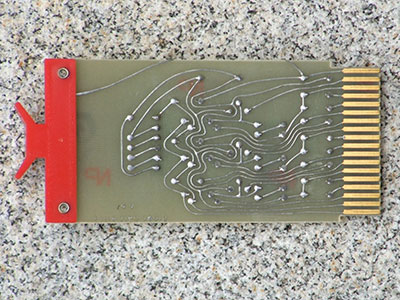
Presensitizing is a PCB manufacturing method that involves the use of UltraViolet (UV) light exposure. It is important to note that the process of Presensitized PCB with UV light is a pleasant and exceptional way of accomplishing a DIY project!
However, before you embark on your project, ask yourself whether you like the concept of a lighter circuit board preparation process and testing with a DIY project. If your heart says yes to the above questions, then it is essential to gain more knowledge about presensitized PCB preparation.
This article digs deep into what is a presensitized PCB, how presensitized PCBs compare with their traditional counterparts, the process of making a presensitized board, and the advantages of presensitized PCBs. Welcome, and let us have fun!
Contents
- 1. What are Presensitized PCB Exactly?
- 2. How do Presensitized PCBs Compare with Traditional PCB?
- 3. How to Make a Presensitized PCB
- 3.1 PCB Artwork
- 3.2 PCB Printing
- 3.3 PCB Preparation
- 3.4 PCB Exposure
- 3.4.1 Use the Easily Accessible Artwork
- 3.4.2 Placement
- 3.4.3 Presensitized PCB--- Insert Your PCB Horizontally
- 3.4.4 Presensitized PCB-- Expose Your PCB for 8 Minutes
- 3.4.5 Presensitized PCB-- Fit the Standoffs
- 3.4.6 Presensitized PCB-- Dip the PCB in Developer Medium
- 3.4.7 Presensitized PCB-- Bathe the Board Severally
- 3.4.8 Presensitized PCB-- Wash with Running Water
- 3.5 PCB Etching
- 4. Advantages of Presensitized PCB
- Final Thoughts on Presensitized PCB
Special Offer: Get $100 off your order!
Please email [email protected] for details.
1. What are Presensitized PCB Exactly?
A presensitized circuit board is a special board with a photosensitive surface coating. It enables you to create a customized design by shifting/burning the image with a UV light. In other words, a presensitized circuit board resembles a standard copper-clad board. The only difference between them is how you transfer the design into the boards.
Special Offer: Get $100 off your order!
Please email [email protected] for details.
2. How do Presensitized PCBs Compare with Traditional PCB?
As mentioned above, the primary difference between a presensitized PCB and a traditional PCB is how you transfer the design into the boards. Basically, this is how you should transfer images in traditional PCBs:
- Toner transfer method
- Inkjet masking method
- By dry film photopolymer method.
On the other hand, you should expose your board to UV light to transfer images in presensitized PCBs. Generally, you add a photosensitive covering during the preparation process. A “peel-off” layer shields the covering from accidental light exposure. Remember to take away the “peel-off” layer before exposing your photosensitive coating to light.
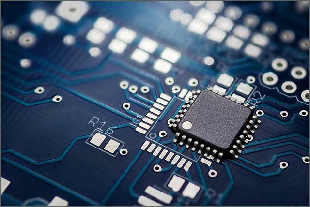
3. How to Make a Presensitized PCB
The first thing to remember is that circuit board printing demands a lot of effort, endurance, and testing! Therefore, bear in mind that you might experience some challenges the first time you design a photosensitive board, leading to errors. For this reason, you should prepare several experimental PCBs if it is your first time.
Besides, it is good to be in touch with a reputable PCB manufacturer to remain confident with the components you are using. This will further ensure your supply chain does not weaken, fade, or become problematic during the manufacturing process.
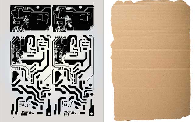
3.1 PCB Artwork
There is a common expression in the computer world that says, “Garbage In, Garbage Out.” The principle applies well with circuit board design. It simply means that your project will only worsen if you begin your project with the wrong artwork.
While there are numerous media you can use to print your circuit board artwork positively, you will get excellent results by printing your artworks on a quality tracing paper.
Remember to scrutinize your tracing paper before utilizing it. Light up one part of the paper with a shiny source of light, and examine it by viewing through the other side. The paper should be free from dark spots and stains. Dark spots cover the artwork portions, forming short circulating pathways around crowded sections of the board artwork.
3.2 PCB Printing
You should use laser-made positive artwork in your PCB printing exercise as they form delicate, crisps, and compact black prints. Inkjet inks seam to stain with tracing paper, resulting in prints with draining and blurry edges. Consequently, this limits the feasible spacing between circuit board pads and traces. Occasionally, bleeding can short circuit narrowly positioned patterns.
3.3 PCB Preparation
It is essential to realize that a presensitized board surface is shielded with a dense grey layer against unintended exposure and impurities. If the layer is still intact, the board can assume irregular treatment during cutting with a slight damage risk. Always remember to keep it intact until you are set for the exposure process.
Chop a board with two contrasting sides, measuring more than 5mm long. You will use the extended part later to attach your PCB standoff clip during the design and etching process. Burrs and uneven edges may limit your artwork from lying ideally uniform. Luckily, you can do away with them using a hand file.
3.4 PCB Exposure
First, clean your exposure box surface with a cloth containing a mild detergent. Then, rinse it with a clean, dry cloth. Remember to keep the surface free from stains and dusty particles to have the most satisfactory image transfer.
You can now set your board for exposure. Note that from this point onward, you should carry out everything under passive light conditions. This is because bright light might accidentally expose your board, essentially hindering your project.
3.4.1 Use the Easily Accessible Artwork
Take out the protective PCB layer. Remember to grasp your board along the edges to avoid touching the exposed parts. Additionally, do not put down the board until you finish the next step.
3.4.2 Placement
Thirdly, gently slide your board in between the upper and lower artwork. Place it accordingly to position and align the artwork at the center of the edges.
3.4.3 Presensitized PCB--- Insert Your PCB Horizontally
Fourthly, insert the board in the exposure box. Place the artwork horizontally and touch the PCB surface to get a refined image transfer. To achieve that, you should place a clear piece of glass on top of your artwork. If you experience loose movements when you apply some pressure, it means that your glass is not lying horizontally. Apply more weight to ensure the glass is horizontal to your artwork. However, remember that heavyweights can break your glass, worsening the situation instead of resolving it.
3.4.4 Presensitized PCB-- Expose Your PCB for 8 Minutes
Turn on the exposure box for an average of eight minutes. The exposure time differs based on the exposure table.
Make the developer medium by mixing three teaspoons of developer powder with one cup of distilled water in a container. Stir the mixture by moderately swinging the container until it dissolves completely.
When the eight minutes are over, retrieve your board from the exposure box, and isolate it from the artwork. Remember to hold it by the edges as you did earlier.
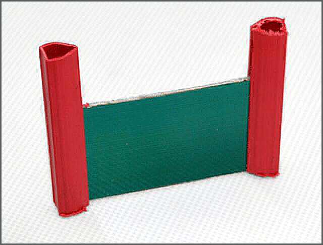
3.4.5 Presensitized PCB-- Fit the Standoffs
Fix the standoff as illustrated below. The standoffs will facilitate the movement of the developer medium on the two PCB sides during bathing. They will also prevent the circuit board surface from polishing with the container surface. If you lack standoffs, you will definitely create a board containing dented patterns.
3.4.6 Presensitized PCB-- Dip the PCB in Developer Medium
Dip your board in the developer medium you prepared earlier. If you are making a single-side board without a standoff, dip your circuit board with the green part facing upwards. The board should be completely immersed in the mixture. You can add more water if you cannot submerge the board entirely.
Gently shake the container to stir the medium. Half a minute into the bath, the artwork you moved should slowly appear on the board surface. If the pattern does not appear, remove the board from the solution and clean it with distilled water.
Then, increase the developer powder and stir to dissolve it completely. Immerse the board back in the solution and examine whether the pattern appears within half a minute. Repeat the process to increase the concentration of the developer powder if necessary.
Continue stirring the bath, and pause after at least 15 seconds to view the exposed copper parts of your board.
3.4.7 Presensitized PCB-- Bathe the Board Severally
If you see traces of green image repels or faint-green pigments in the exposed surface, know that you still have unfinished business. Bathe the board once again until you only remain with the board pattern. Once you are satisfied, you can continue bathing the board for another one minute to dissolve any undesirable image resists you might have neglected during the examination.
3.4.8 Presensitized PCB-- Wash with Running Water
Lastly, wash the board well with running distilled water. Wow! Your circuit board is now set to undergo the etching process.
3.5 PCB Etching
PCB etching is an important step in the chemical preparation of presensitized PCBs. It involves the removal of copper to obtain desirable patterns. Remember, you need to do away with every copper residue apart from the circuitry covered by the tin plating.
PCB etching seems to be a complicated process for some people, but actually, it is not a challenging activity, as you may think. After collecting all the necessary materials, print your layout before printing the circuit layout. Sketch your design in transparent acetate material to achieve the desired results.
Use a laser printer instead of an inkjet printer to print your acetate. We prefer printed ink on acetate because it does not stick; hence, you will not get undesired results. Alternatively, you can use a laser printer toner. But if you do not have a laser printer, you can make good use of an acetate photocopy.
It would be best to dissolve a developer powder in warm water to form a universal circuit board developer. Most etching agents, like ferric chloride, come in powder or solution form. In the case of dust, apply the same approach with the developer powder.
You can watch this video to gain a better visual illustration of how to prepare presensitized PCBs
https://www.youtube.com/watch?v=3ApEYfZPX8o&feature=youtu.be.
4. Advantages of Presensitized PCB
Presensitized PCBs have numerous benefits, making them the number one choice of most manufacturers and engineers. Below are the main advantages of presensitized PCBs.
- The main advantage of presensitizing is that it is more accurate than other circuit board processing approaches, like the toner transfer technique.
- The process of presensitization is also very cost-effective. Presensitization excludes fabrication steps, lowering expenses. Therefore, you can experiment with your creative concepts without distressing about going beyond your budget limits.
- Presensitized circuit boards are dense, minimizing the use of several wires on a board. They use interconnections to link parts via copper tracks, unlike the use of multiple cables to conduct current in traditional circuit boards. With presensitized circuit boards, the interconnections are somewhat less immense.
- Presensitized circuit boards are easy to repair in case they break down. Additionally, they are easy to examine and consequently replace individual failure components. This is because manufacturers design and label the electronic parts and polarities present in presensitized boards accurately.
- Presensitized PCBs also save much time during assembling. You will take more time to connect components in traditional PCBs. On the other hand, you will take less time to connect components of presensitized PCBs. This is why many engineers love them.
- Most presensitized boards are resistant to movement. If you are a keen individual, you will realize that most presensitized circuit board components contain strong grips. They employ solders, which limit their movement regardless of the direction of the PCB to achieve stability.
- Presensitized PCBs are highly reliable compared to traditional PCBs. Talking about reliability and performance, presensitized boards provide desirable results. This is also another reason why most electrical engineers choose them over their traditional counterparts.
Final Thoughts on Presensitized PCB
Congratulations! We trust that you have gained a better understanding of presensitizing circuit boards. You must have also realized that making custom PCBs is a unique, enjoyable, and cost-effective approach to experiment with DIY projects.
It is undeniable that making PCBs is one of the most admirable skills in the electronic world. Mastering this essential skill can save you a lot of frustration, time, and resources. And we cannot forget the abundance of fun you enjoy throughout the process.
Do you need professional help with your custom PCB designing process? We are willing to offer a lending hand to all PCB hobbyists in their DIY projects. If you require assistance throughout your PCB production process, we are your one-stop solution for all your PCB manufacturing needs. Remember, your project deserves quality materials and a professional support team to succeed. We have got you covered in all these.
Special Offer: Get $100 off your order!
Please email [email protected] for details.