Electronic devices feature printed circuit boards that begin as PCB designs before fabrication. Traditionally, contract manufacturers relied on Gerber files created by Computer Aided Design systems to get PCB designs, but these have serious drawbacks. For instance, they lacked critical information that prompted delays between design and manufacturing. ODB++ came into the market to solve these issues. This article looks at ODB++ and how it is better than the Gerber file format. Take a look!
Contents
Special Offer: Get $100 off your order!
Please email [email protected] for details.
What is ODB++?
ODB++ means Open Database ++ and is a CAD-CAM data exchange format used in PCB assembly, development, and manufacture. Combining the files creates a design from a single concept for the entire board manufacturing process. In other words, the file format contains all the required design information to prevent data misinterpretation and errors in PCB manufacturing.

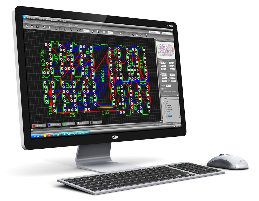
An electrical engineer designing a PCB using CAD software
You can transfer the ODB++ PCB design information between design and production and among the design tools from different CAM and CAD software vendors. It is worth mentioning that ODB++ design, ODB++ process, and ODB++ manufacturing are the latest file formats.
ODB++ File Structure
Even though ODB++ data comes as a single file, it is a framework containing directory files zipped using gzip. Therefore, the file format consists of a hierarchy of files and folders joined to form a standard file system structure.
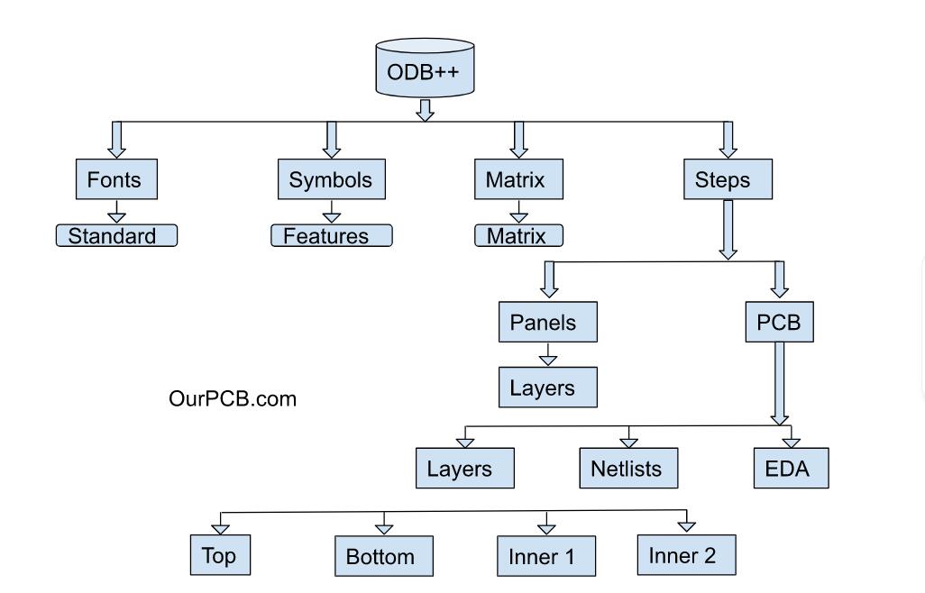
ODB++ file hierarchy
One of the best features of the format is that all the files are ASCII readable. Therefore, advanced users can read the Open Database files directly without requiring any specialized extraction program.
Most legacy systems used binary database files that required special format conversion software. Vendors preferred these databases due to limited disk space, but hard disk capacity has increased drastically.
On top of that, efficient compression techniques have emerged to help reduce the size of ASCII databases. Large files in ODB++ get stored in the standard UNIX compress format.
Importance of CAD and CAM in PCB Fabrication
PCB fabrication begins with the product design process, and Computer Aided Design software packages help create the PCB designs, which are virtual representations of PCBs.
Besides design, other useful CAD software features include design reuse, auto-routing, 3D visualization, and data management.
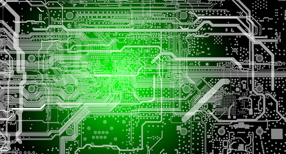
A 3D render of a PCB design on CAD software
After finalizing and verifying the printed circuit design, the file goes to the CAM (Computer Aided Manufacturing) processor. The CAM processor's purpose is to realize the virtual design into a physical product.
A uniform data exchange protocol will be absent if different companies design the CAD and CAM files. The development of several CAD-CAM data exchange protocols solved this issue. These protocols function as bridges between the incompatible CAD and CAM systems, one of them being ODB++.
Special Offer: Get $100 off your order!
Please email [email protected] for details.
ODB++ Family
The ODB++ data format has undergone modifications to simplify the printed circuit board design and manufacturing processes. The result of this modification is the ODB++ family, a package consisting of the following.
ODB++ Design
These files contain the printed circuit design information for the board, and you can create them using any EDA software. They form the basis for conducting any DFM, DFA, and other similar tests.
Designing the inner layers of a PCB (PCB layout routing)
ODB++ Process
Production machinery or equipment needs the design data in a machine-readable format. The ODB++ process file does the machine translation for the equipment to read the data and do the required action.
ODB++ Manufacturing
These files are one step above their ODB++ Process counterparts. They provide the required input for manufacturing floor events and create a communication channel between the machinery and intelligent industry software.
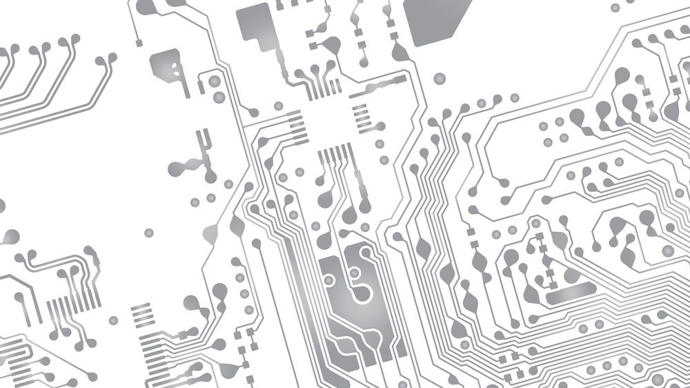
Gerber vs. ODB++
ODB++ and Gerber are the two top data exchange formats used in PCB design and manufacturing. Gerber is often considered the industry standard as it is more typical in designing PCBs in the industry.
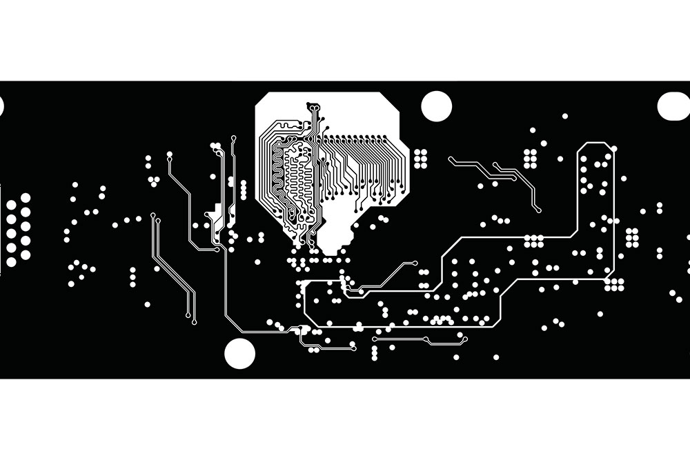
A PCB layout with Gerber files of the inner layers
However, ODB++ is giving Gerber a run for its money and is quickly becoming the de facto board format design in PCB fabrication due to its superior accuracy and performance.
Although Gerber holds about 90% of the market share, it has critical limitations, such as lacking layer stack up and drilling information. These limitations can cause inaccurate copper layer ordering and increase the risk of missing holes.
The ODB++ format eliminates the need for using multiple CAM and CAD files by providing one hierarchical structure with all the data. This information includes the drill & layout information, plus details about the dimensions, BOM, fabrication, and testing.
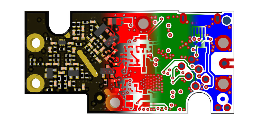
A PCB design concept blended with Gerber files of the inner layers
The comprehensive data minimizes the risk of machine & human errors. Additionally, it increases the speed and turnover time because it allows a high degree of automation.
Data Obtained from ODB++
Every compressed ODB++ file contains information you can insert directly into the front-end CAM system. This CAM system then outputs the programs to run the process equipment efficiently.
A grayscale PCB data transfer infographic design
PCB Manufacturers usually make tiny adjustments in consultation with customers to maintain design integrity. For instance, if the pad is not large enough or there is insufficient spacing, the design needs a minor edit. The system then checks these edits automatically against the netlist to confirm the change does not affect other areas.
Why Circuit Board Manufacturers Prefer ODB++ Over Gerbers
- All the data required for PCB production, assembly, and testing come in a single file
- Reduced risk of transmission errors
- Reduced delays in communication between the designer and manufacturer
- Integrated DFM (Design For Manufacturing) support available in all layer types
- Allows a high level of automation in all PCB production phases
- Supported by all major DFM, CAD, and CAM tool manufacturers
ODB++ Benefits
- Reduces supply chain risks caused by transmission errors
- Differentiates between pad and conductor, unlike the Gerber standard format
- It contains a complete layer table that defines the original layer name, layers orders, and layer type
- The comprehensive file structure (hierarchy structure) minimizes machine and human errors
- Allows testing point and fiducial definition using an attribute system
- Supports flexible and rigid-flex PCBs
Wrap Up
In conclusion, ODB++ solves most of the issues presented by the Gerber file format. Although not as popular as Gerber, the data exchange file format is increasingly becoming the preferred option by designers and contract manufacturers due to its all-in-one information hierarchy structure. That's it for this article. Thanks for your reading.
Special Offer: Get $100 off your order!
Please email [email protected] for details.