All components in a PCB need electrical power to function. So you need to design the electrical lines and loads in the circuit to create an effective power distribution network.
Similarly, you should supply the correct electrical current and voltage to all areas on the board.
There is also the issue of power integrity, which is critical for the board. Let’s look at what power distribution networks are all about below.
Contents
- Factors to Consider When Designing a PDN
- Voltage Supply
- Current Supply
- Routing Power To Components
- Block Diagram for Power Distribution Networks
- What About Power Integrity?
- Electromagnetic Interference (Noise)
- Ground Bounce
- Power Ripples
- PDN Analysis
- How To Analyze a PDN
- Steps for Designing an Efficient PDN
- PCB Design Guidelines for Power Distribution Networks
- Layers/Stack
- Power/Ground
- Capacitors
- Vias
- Others
- Wrap Up
Special Offer: Get $100 off your order!
Please email [email protected] for details.
Factors to Consider When Designing a PDN
The three vital things to consider when designing a board’s PDN are:
- The voltage required by components
- Current draw by components
- Power Routing
Voltage Supply
Chips and components can have different voltage requirements, but the most typical level is 3.3V.
So generally, the voltage across the board should be at this level. If some chips or components require 5V, incorporate a DC-to-DC converter in the circuit.
Also, you should determine if the required voltage is in AC or DC before selecting the board’s power supply.
If the board requires both electrical currents, you can use an AC power supply to power the AC components first.
After that, you’ll need a converter (rectifier) to convert some of the energy to DC to run the other parts.
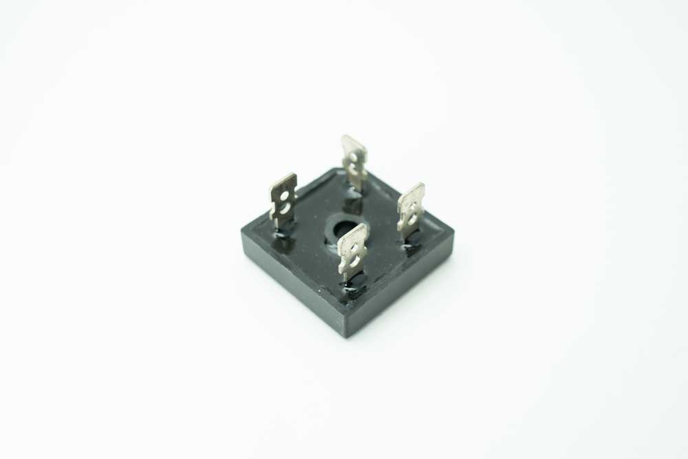
A bridge rectifier
Current Supply
Usually, the sizable through-hole components are more power-hungry than their smaller SMT counterparts.
So you’ll need to calculate the regular current consumption of all electrical components to determine the power supply you’ll use.
And it is best to compute the peak current consumption for each part.
Remember, power supplies have limits on the maximum amperage they can provide.
But instead of oversizing the power supply to handle the peak current, you can use capacitors. They are cheaper.
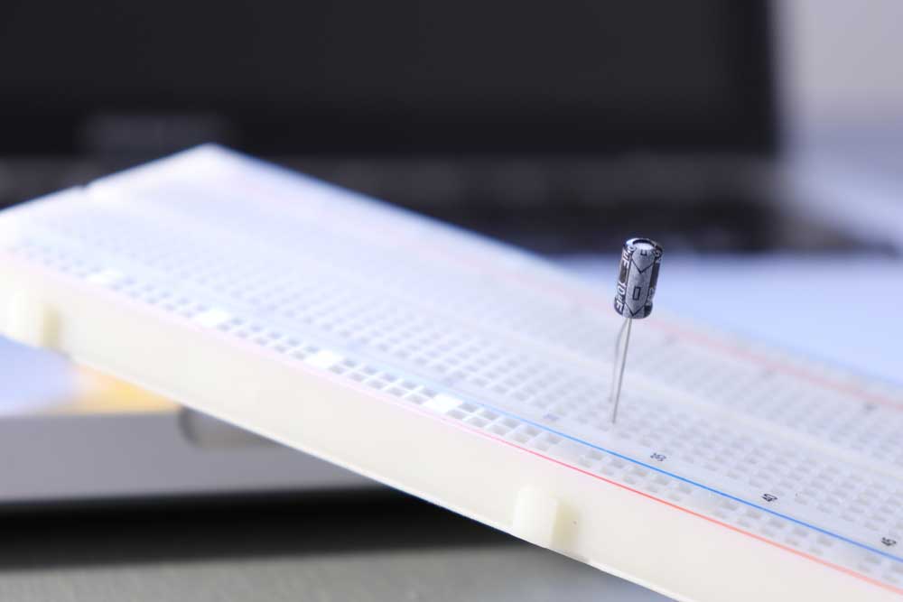
An electrolytic decoupling capacitor
Capacitors will store charge when components operate at normal levels, then discharge when current consumption spikes.
So ensure the capacitor is large enough to hold enough charge to cover the peaks.
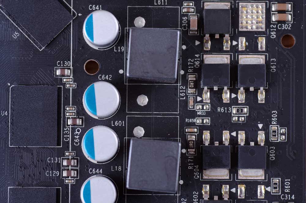
Routing Power To Components
Once you’ve sorted the voltage and current requirements, the next step is to get the power to the components.
And ensure you get the trace width factor right. Space is valuable in circuit boards, so make the conductive tracks as thin as possible.
But if overly thin, they will restrict the current flow. So the components will not get the required power, and the tracks will heat the board (resistance).
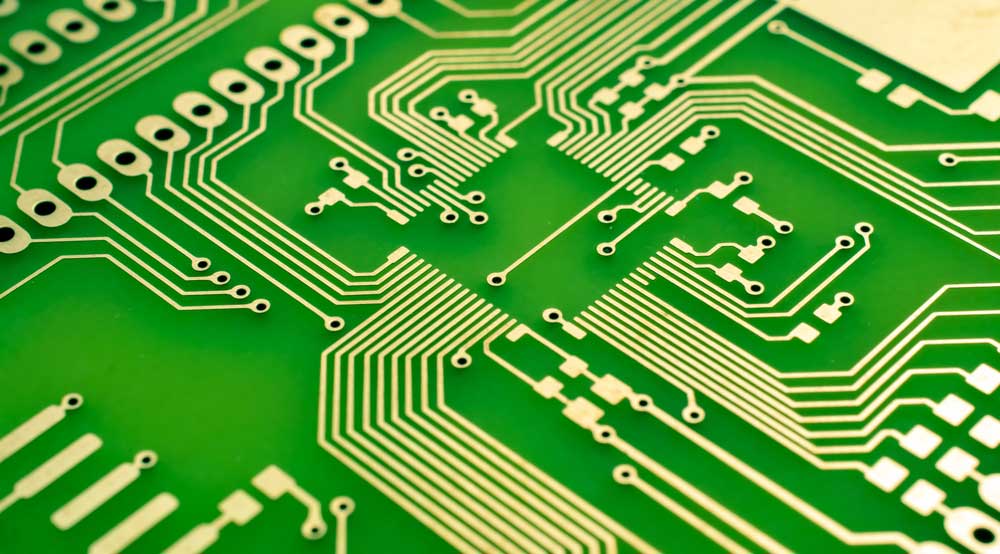
Conductive tracks on a PCB
However, it might be impossible to eliminate the heating effect caused by high current densities in the tracks in some cases.
So check for potential hotspots during the design phase and find ways to prevent board failure.
And if using low-power chips on the board, voltage drops can occur.
Usually, the voltage from the source drops when transmitting the power through long, thin traces with high current densities.
So calculate this drop and broaden the trace width to ensure the chips get the required voltage.
Block Diagram for Power Distribution Networks
Considering the two factors above, a power distribution network has this block diagram.
The VRM (Voltage Regulator Module) is usually a buck converter that converts high voltage levels to lower ones.
Such low voltages (3.3V or 5V) are enough to power chipsets and microprocessors on the PCB.
And in the most basic form, you can represent the PDN using an R-L-C network.
Similarly, you can define the network’s impedance (Z) using a combination of resistance, inductance, and capacitance.
- Resistor: Z = R
- Capacitor: Z = 1/jωC
- Inductor: Z = jωL
This R-L-C component can be in series or parallel, as shown below.
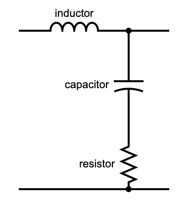
An R-L-C component connected in series
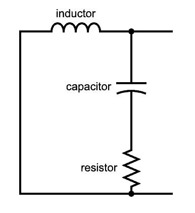
An R-L-C component connected in parallel
So a simplified PDN network resembles the block diagram above but with these R-L-C components.
From this diagram, you can see the PDN is a multiport network. And switching components on the buses can affect the power distribution.
Special Offer: Get $100 off your order!
Please email [email protected] for details.
What About Power Integrity?
On the early simple circuit boards, integrated circuits used to have a single power and ground pin with long traces.
But as circuit densities increased and boards became smaller with multiple layers, the power requirements and distribution became more complex.
The complexities arise from these three issues.
Electromagnetic Interference (Noise)
Electrical circuitry has become more susceptible to noise from internal and external components as frequency increases.
Even the signal, power, and ground nets can create interference.
The typical culprit is the quick signal transition (high to low) on various device internal circuits and I/Os.
So the higher the frequency bandwidth and magnitude, the more the noise.
And this noise can affect the power distribution network, causing several internal problems.
For instance, if this noise exceeds a particular threshold, it can affect the voltage supply to integrated circuits. This situation will cause malfunctions.
But you might still get issues even if the noise does not exceed the threshold. It can create crosstalk in the signal lines or move to the input power source line.
From there, the noise can travel to other VRM inputs and come out on the other end.
A voltage regulator module on a graphics card
Lastly, PDN connections are usually the broadest on printed circuit boards because they carry the highest electrical currents.
So high-frequency PDN noise can produce high electromagnetic radiation, causing the board to fail EMC compliance tests.
Ground Bounce
Also known as simultaneous switching noise, a ground bounce occurs when multiple digital signals change states concurrently.
This situation usually occurs if memory/data buses fail to return current to their signal grounds due to fast switching.
The unwanted circuit noise can lead to accidental switching that causes device malfunction.
And when the electrical current gets pulled into the power distribution network, it causes ground bounce.
So the ground voltage will rise from zero while the positive line remains constant, affecting the circuit’s potential difference.
Power Ripples
Power ripples occur when a transient current propagates voltage fluctuations in the positive PDN rail.
So they create noise because the voltage in this line does not match the output signal from the rectifier.
These ripples will create crosstalk in other circuits, degrading the signal quality.
Modern integrated circuits have multiple power and ground connections.
For instance, large chips, such as those with BGA packages, have hundreds of power and ground pins with different references.
So they usually have a high current draw.
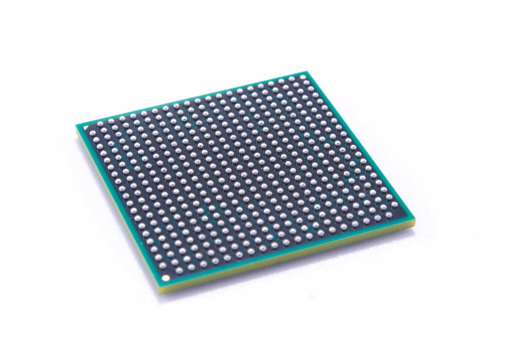
A ball grid array semiconductor chip
Therefore, you should ensure the electrical current supply to these chips does not have ripples, spikes, or noise.
And the only way to achieve that is to design an efficient PDN.
PDN Analysis
You need these inputs to extract PDN performances from PCB layouts.
- PCB schematic diagram
- Board stack-up with Dk and Df dielectric properties
- PCB layout
- Power integrity tool
- S-parameters capacitor models direct from the manufacturer
And since various factors can impact the board impedance, you can evaluate it from these two perspectives.
- EM field solvers
- Circuit simulators (consider interplane capacitance and capacitor self-resonance)
How To Analyze a PDN
The best and easiest way to analyze a power distribution network is by using a PDN analyzer.
This tool gives a visual display of the PDN, enabling you to get insights into the potential problems in the design phase.
It saves you the time and cost of manufacturing faulty boards, which will require a redesign after prototyping.
Some of the issues the PDN analyzer can display include the following.
- Isolated copper areas
- Excessive copper
- Insufficient copper
- Marginal voltages on the device power pins
- Uncontrollable voltage drops
Steps for Designing an Efficient PDN
- Determine the highest signal frequency while considering the fastest signal rise time.
- Formulate the target PDN impedance for every power rail.
- Sketch the PDN (a simplified version), and calculate the impedance and different frequencies.
- Plot a PDN impedance spectrum using the computed value above. This spectrum should help you understand how decoupling capacitors and conductor/via geometry affect the PDN.
- Pick the most appropriate decoupling capacitor and conductor/via geometry. Ensure the PDN impedance is less than the target PDN impedance for each power rail across the operating frequency spectrum.
PCB Design Guidelines for Power Distribution Networks
Getting the PDN impedance to be less than the target PDN impedance is not easy. So follow these tips to get the PDN impedance as low as possible.
Layers/Stack
- Design a board with a symmetrical layer stack up (mirror the top layers in the bottom)
- Ensure the core and prepreg layers have the same thickness
- Verify with your PCB manufacturer if they can fabricate your layer stack up before committing to it
Power/Ground
- Assign the ground and power layers first while ensuring they are as close as possible
- Try to keep the power and ground planes symmetrical in the stack to maximize signal integrity
- Place the high-density copper layers in the middle of the stack
- Use the same copper weight in the plane layers
- Don’t share conductive tracks for nets that are highly noise sensitive
- Implement a fanout strategy to reduce the return path (to curb loop inductance)
- Place several parallel return paths in the power ground
- Avoid designing loop inductance paths
- Place tiny islands for power rails. Alternatively, design broad traces to match the current draw
- Decrease inductance or increase capacitance to minimize voltage response to transient current steps
Capacitors
- Place decoupling capacitors after the primary components to increase capacitance and reduce inductance
- Use different capacitor values to flatten the impedance profile
- Position the decoupling capacitors on the top and backside for optimization
- Place decoupling capacitors in all power rail pins and link them using through-hole vias if on the other board side
Conductive traces linked to through-hole vias in a circuit board
Vias
- Avoid Via sharing; use Via on pads instead
- Link the same nets using Vias. Use staggered Vias if buried or blind
- Position four through-hole Vias on the corners of ICs to shorten the return path
Others
- Use copper planes for heat dissipation
- Confirm the minimum anti-pad your PCB manufacturer can build reliably (adjust that to your design to reduce DC resistance)
- Prioritize board floor planning from 50-60% completion of the schematic completion
Wrap Up
Designing effective power distribution networks requires technical voltage, current, inductance, impedance, and circuit design knowledge. So it is not easy.
Therefore, we recommend getting a professional to help you design a PDN if you are rusty.
And even if you have done the design, you should get your PCB manufacturer to analyze it.
At OurPCB, we have the required expertise and equipment to examine your layouts.
So contact us today to get this technical assistance. We’ll be happy to help.
Special Offer: Get $100 off your order!
Please email [email protected] for details.