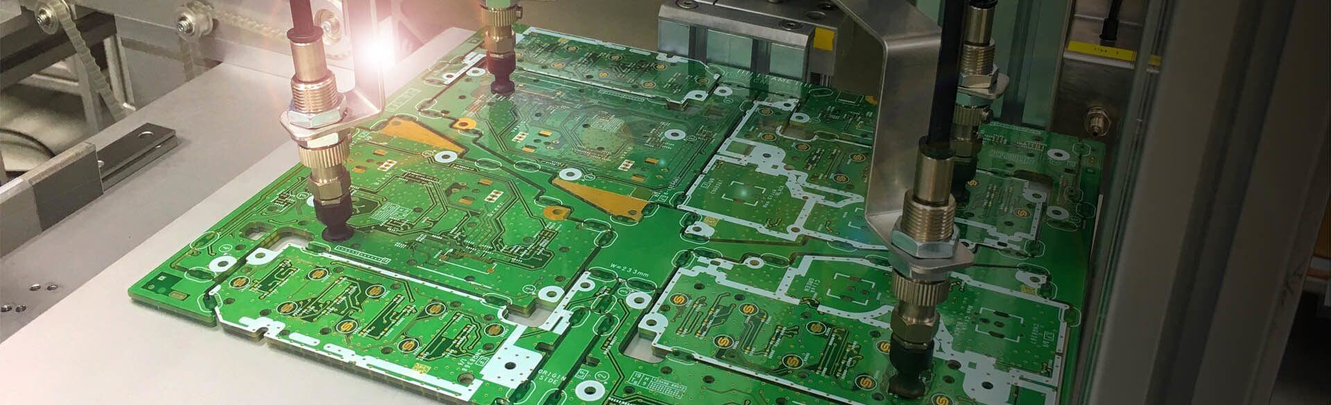
OURPCB’s dedicated pcb prototyping facility is a full turnkey, fast turnaround, high technology service.
PCB Prototyping Features:
♦ Layers: 1-32
♦ Finished Copper: 0.5-5oz
♦ Min. Line/Track Width: 3mil.
♦ Min. Line/Track Space: 3mil.
♦ Finished Board Thickness: 0.2-5.0mm.
♦ Min. Finished Diameter of PTH Hole: 0.2mm.
PCB Prototyping Standard Lead time:
♦ 1—2layers:5days
♦ 4layers:6days
♦ 6 layers:7days
♦ 8layers:8days
♦ 10layers:9days
♦ 12 layers:11days
♦ *Shipping time is not included
PCB Prototyping Payment:
♦ Paypal is acceptable
♦ Cash on Delivery is acceptable
PCB Prototyping Service:
♦ Formal quotation in 8 working hours.
DHL, FedEx, TNT, EMS are available