

We employ professional engineers and have strict quality control for each process.
The quality assurance department is in charge of testing all products before they are sent to the customer.
This includes AOI test, X-RAYs, and E-test which ensures that there will be no issues with your product once you purchase it.
We're committed to providing you with the highest quality products and services at competitive prices (especially multilayers PCBs).
Special Offer: $1 for 5 PCB Assemblies!
Please email [email protected] for details.
ABOUT HEAVY COPPER PCB
A heavy copper PCB is a board that uses up to 20 ounces of thick, heavy-duty copper. This type of circuit undergoes special etching and plating methods like differential etching and step plating. You can also call it a “thick” or “heavy” Copper PCB (copper weights range from 4 oz/ft2 to 20 oz/ft2).
Copper is a great conductor for electricity, which means that it can handle high-current/high-power circuits and control circuits on the same board.
And it’s possible to integrate control circuits and high-power circuits on the same board. Plus, it comes with different perks like cost-effectiveness (long-term), low impedance power distribution, etc.
BENEFITS OF THICK COPPER PCBS
You could use these heavy copper-deposited parts of the board as heat sinks.
The copper board transfers heat to the heatsink, and that's possible thanks to its plated vias. The higher current can be transmitted.
The board can withstand high temperatures and has a long lifespan.
The board protects against circuit failure protects the sensitive parts of your electronics from dust and debris.
The PTH holes and connector sites on the board have high mechanical strength.
The board has a high level of resistance to thermal strains.
The PCB is perfect for any size project with different copper weights. The weight of the circuit board and its layers is equally weighted, making it a great versatile option!
Heavy copper PCBs carry heavy current throughout the board for all of your power needs.
The Heavy Copper PCB’s lack of complex wire bus configurations is a great way to save time and money on production.
Our Heavy Copper PCB comes with exotic materials. These materials are useful for enhancing the board’s mechanical characteristics and can also improve electrical efficiency, cutting-edge power delivery circuits, and heat dissipation capabilities.
HEAVY COPPER PCB/ THICK COPPER
PCB CAPABILITIES
We are one of the leading producers in China and have experience with thick PCBs that is unrivaled.
Considering this, here’s an informative table about how much capacity our factory has:
Special Offer: $1 for 5 PCB Assemblies!
Please email [email protected] for details.
OURPCB
One thing you can be sure of about heavy copper PCB: it requires the best technology to produce reliable results. Despite the challenges involved in its fabrication, we deliver quality at a competitive price point.
Plus, we have been in the business for years. So not only can you count on our experience to build your dream PCB based on your specifications, but it also means that whatever small or large volume of boards you need to be built and assembled is taken care of by us as well!
HEAVY COPPER PCB DESIGN PROCESS
Before diving into the design process of thick copper PCB, it’s crucial to consider parameters like:
This will help you save time and money in your production.
The spacing
The type of parts
Ideal dimensions
Here is a table that summarizes the dimensions:
| Criteria | Baseline thickness of copper foil | |||
|---|---|---|---|---|
| 105μm | 140μm | 175μm | 210μm | |
| Loss (mils/mm) | Ca. 3 / 0.08 | Ca. 5 / 0.13 | Ca. 6 / 0.15 | Ca. 7 / 0.18 |
| Minimum spacing (mils) | 13 | 15 | 20 | 27 |
| Minimum path width (mils) | 12 | 14 | 18 | 25 |
With these parameters in mind, you can do the following:
1.So. A few ways to avoid this is by checking the copper fill levels in your boards. You can tell if there will be any problems with voids and delamination is by watching for deficient fill levels, which happens when resins are low.
2. If you want to achieve a multilayer build-up design, selecting your preg numbers and types with software.
3. The galvanic coating is important. And considering that you’re dealing with a heavy copper PCB, the amount of galvanized copper topcoat required will be more than what’s needed for your average circuit board.
4. Thick layers of solder resist will keep the mosaic edges safe. For example, your final circumferential thickness should be at least 0.25mm higher than its initial thickness.
FAQS OF THICK COPPER PCB
1. How thick is the copper on a PCB?
The copper thickness in PCB boards is usually determined by the amount of copper used. The standard layer has about 1 ounce, which translates to 35 micrometers thick. But a finished product should have 2 ounces or 75 millimeters thick.
2. How do you choose the thickness of PCB copper?
Many factors determine what thickness of PCB copper you choose. It would help if you considered the operating temperature, how long it would be exposed to heat, and any chance for a circuit board failure to avoid damage.
3. How do you remove unwanted copper from a PCB?
To achieve the best result, etching is subtractive. It would help if you had a temporary mask for your PCB and use acid to remove unwanted copper from it while other parts are protected.
4.Why is copper used in PCB?
Copper is the most popular metal for a PCB because it transmits signals effectively and doesn’t lose electricity in the process.
5.What is the base copper weight?
Copper is typically the material used for plating on PCBs. Base copper weight refers to the quantity of this metal present before it is covered with other components like solder, flux, and epoxy.
HEAVY COPPER PCB
More PCB SERVICES
product
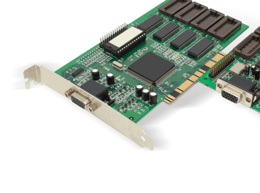
PCB Assembly
product
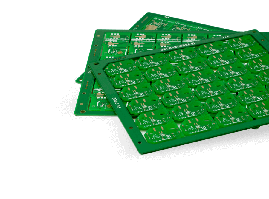
PCB Manufacturing
product
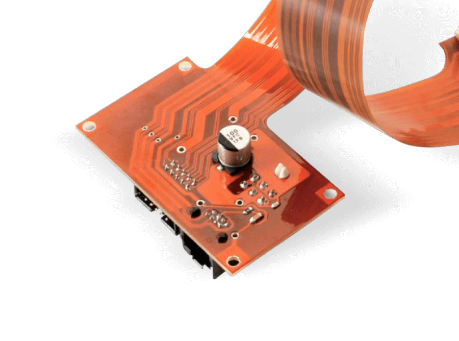
Flexible PCB
product
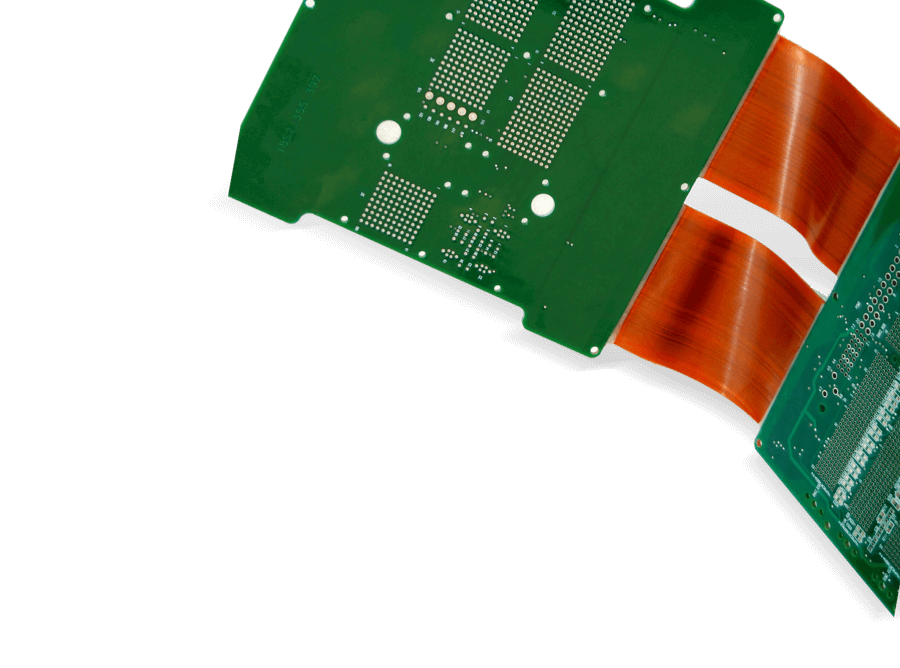
Rigid-Flex PCB
Special Offer: $1 for 5 PCB Assemblies!
Please email [email protected] for details.